InGaN diode-laser pumped II-VI semiconductor lasers

Active Publication Date: 2005-12-15
COHERENT INC
View PDF12 Cites 25 Cited by
  • Summary
  • Abstract
  • Description
  • Claims
  • Application Information

AI Technical Summary

Benefits of technology

[0006] In one aspect, a semiconductor laser in accordance with the present invention comprises a multilayer semiconductor laser heterostructure including at least one active layer of a II-VI semiconductor material having a formula AxB1-xCyD1-y, where x is equal to or greater than zero and less than or equal to one, y is equal to or greater than zer

Problems solved by technology

These lasers, unfortunately, have been found to have rela

Method used


Image

  • InGaN diode-laser pumped II-VI semiconductor lasers
  • InGaN diode-laser pumped II-VI semiconductor lasers
  • InGaN diode-laser pumped II-VI semiconductor lasers

Examples


Embodiment Construction

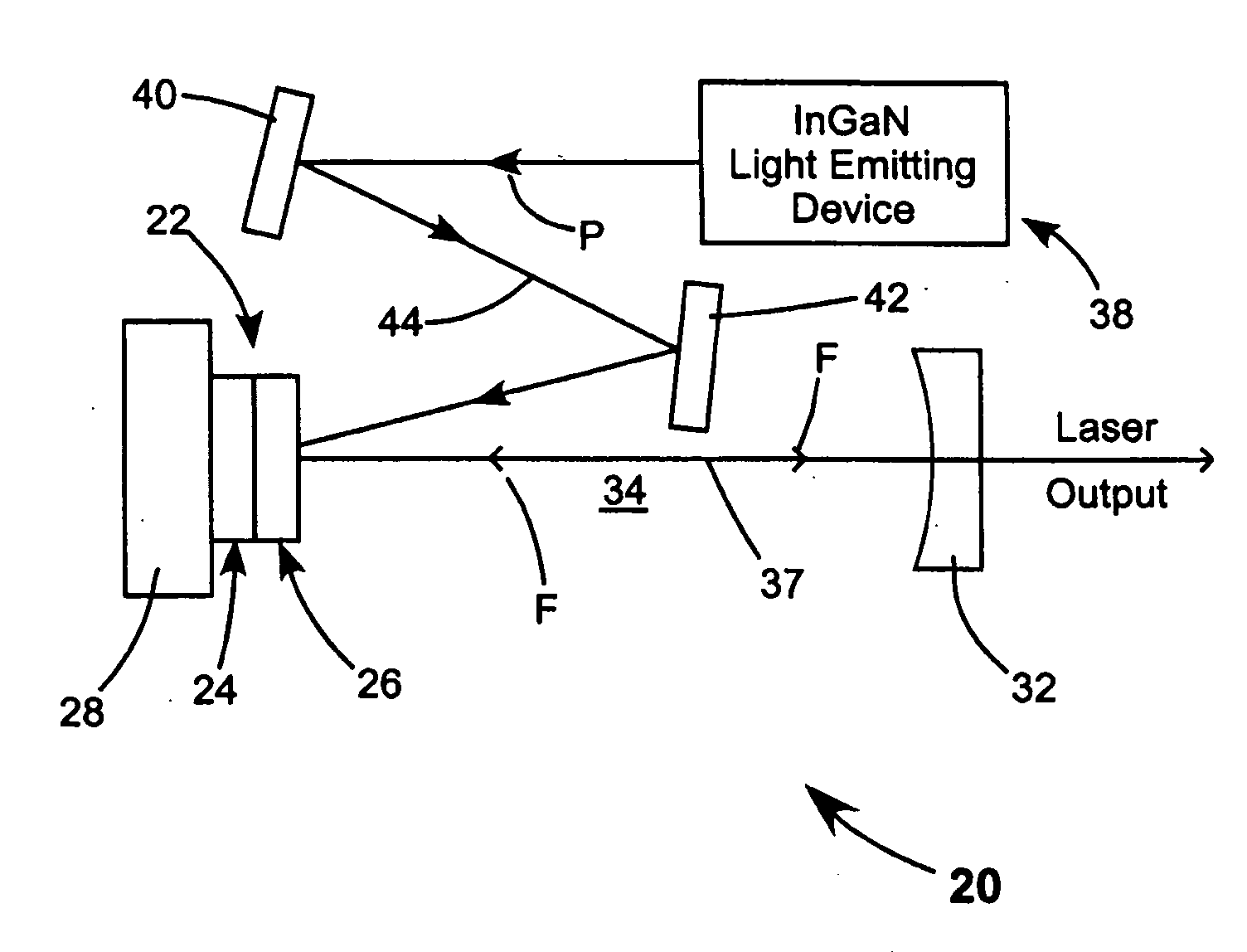
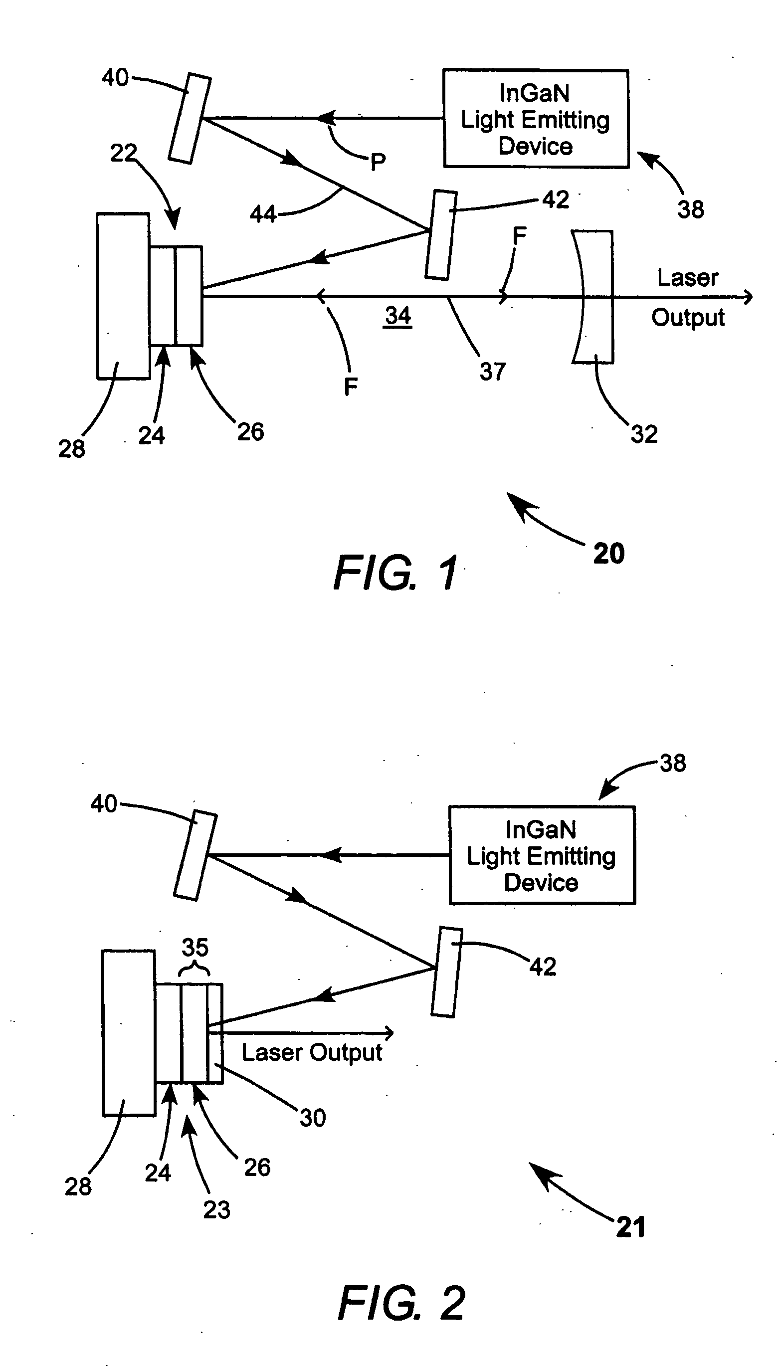
[0018] Referring now to the drawings, wherein like components are designated by like reference numerals, FIG. 1 schematically illustrates one embodiment 20 of a II-VI semiconductor laser in accordance with the present invention. Laser 20 includes a surface-emitting semiconductor heterostructure 22 including a mirror structure 24 surmounted by a gain-structure 26. Heterostructure 22 is in thermal contact with a substrate, heat sink, or heat spreader 28. Substrate 28, optionally, may be a substrate on which the heterostructure is grown.

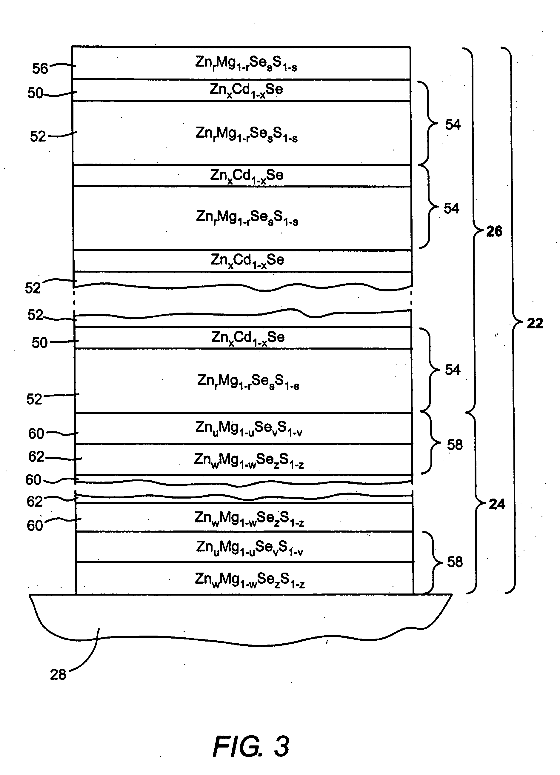
[0019] Gain structure 26 includes a plurality of active layers of a II-VI semiconductor material having a formula AxB1-xCyD1-y, where x is equal to or greater than zero and less than or equal to one; y is equal to or greater than zero and less than or equal to one; where A and B are selected from a group of group II elements consisting of (Zn, Cd, Mg, Be, Sr, and Ba); and where C and D are selected from a group of group VI elements consisting of (S, Se...


PUM


Abstract

A semiconductor laser includes a multilayer semiconductor laser heterostructure including at least one active layer of a II-VI semiconductor material and is optically pumped by one or more indium gallium nitride (InGaN) diode-lasers. Group II elements in the II-VI semiconductor material are zinc, cadmium, magnesium, beryllium, strontium, and barium. Group VI elements in the II-VI semiconductor material are Sulfur, Selenium, and Tellurium. In one example of the laser an edge emitting heterostructure includes two active layers of zinc cadmium selenide, two waveguide layers of zinc magnesium sulfoselenide, and two cladding layers, also of zinc magnesium sulfoselenide. Proportions of elements in the cladding layer material and the waveguide layer material are selected such that the waveguide layer material has a higher bandgap than the material of the waveguide layers. In another example, a two dimensional array of InGaN diode-lasers is arranged to optically pump a one dimensional array of II-VI edge-emitting heterostructure lasers.

Description

TECHNICAL FIELD OF THE INVENTION [0001] The present invention relates generally to semiconductor lasers. The invention relates in particular to semiconductor lasers grown from II-VI semiconductor materials and emitting in a blue region of the visible electromagnetic spectrum. DISCUSSION OF BACKGROUND ART [0002] One potential application for semiconductor lasers is in the illumination of color display devices. In any such device wherein it was desired to provide an accurate color display, it would be necessary to provide at least one semiconductor laser emitting red light, at least one other semiconductor laser emitting green light and at least one further semiconductor laser emitting blue light. [0003] Most commercially available blue-light emitting diode-lasers are made from indium gallium nitride (abbreviated InGaN), a II-V semiconductor having a general formula InxGa1-xN, where x is equal to or greater than 0.0 and less than or equal to 1.0. The lasers can be made to emit at a pa...

Claims


Application Information

Patent Timeline
IPC IPC(8): H01S3/0941H01S5/00H01S5/04H01S5/14H01S5/183H01S5/343H01S5/347H01S5/40
CPCB82Y20/00H01S3/094057H01S3/0941H01S5/005H01S5/4025H01S5/141H01S5/183H01S5/34333H01S5/347H01S5/041
Inventor SPINELLI, LUIS A.ZHOU, HAILONGAUSTIN, R. RUSSEL
Owner COHERENT INC
Why Eureka
Try Eureka