Temperature stable metal nitride gate electrode

a metal nitride and gate electrode technology, applied in the direction of semiconductor devices, semiconductor/solid-state device details, electrical devices, etc., can solve the problems of gate leakage current becoming unacceptably high, reducing the capacitance of the gate, and affecting the performance of the device, so as to reduce the polysilicon depletion

Active Publication Date: 2005-12-22
GLOBALFOUNDRIES US INC
View PDF10 Cites 19 Cited by
  • Summary
  • Abstract
  • Description
  • Claims
  • Application Information

AI Technical Summary

Benefits of technology

[0010] The present invention provides a gate structure for a CMOS device that offers temperature stability, a substantially reduced polysilicon depletion effect, and numerous other advantages. This gate structure has a metal nitride layer in contact with the gate dielectric, where the nitrogen concentration in the layer is increased.

Problems solved by technology

The ongoing reduction in size of electronic device elements poses problems in device performance which must be addressed using new materials and fabrication techniques.
If a conventional oxynitride gate dielectric is used, decreasing the thickness below about 1.2 nm (equivalent oxide thickness) causes the gate leakage current to become unacceptably high.
The appearance of this depletion region reduces the capacitance of the gate and thus increases the electrical thickness.
If a gate structure about this size is designed with a gate dielectric equivalent thickness of about 1 nm, a conventional oxynitride gate dielectric can no longer be used due to unacceptably high leakage currents.
However, the combination of polysilicon for the gate conductor 11 with a high-k material for the gate dielectric 12 presents further problems.
In particular, an increased Vt may prevent proper function in a PFET.
Another problem affecting PFET performance is that of penetration of boron from the p+ type polysilicon into the high-k dielectric and possibly into the channel region of the device; this effect renders the device unusable.

Method used


Image

  • Temperature stable metal nitride gate electrode
  • Temperature stable metal nitride gate electrode
  • Temperature stable metal nitride gate electrode

Examples


Embodiment Construction

[0030] Temperature-Stable Gate Structures

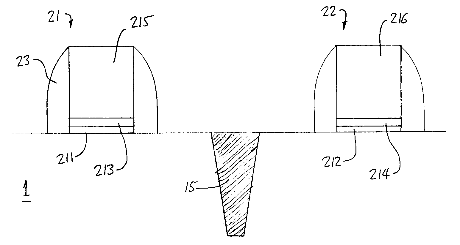
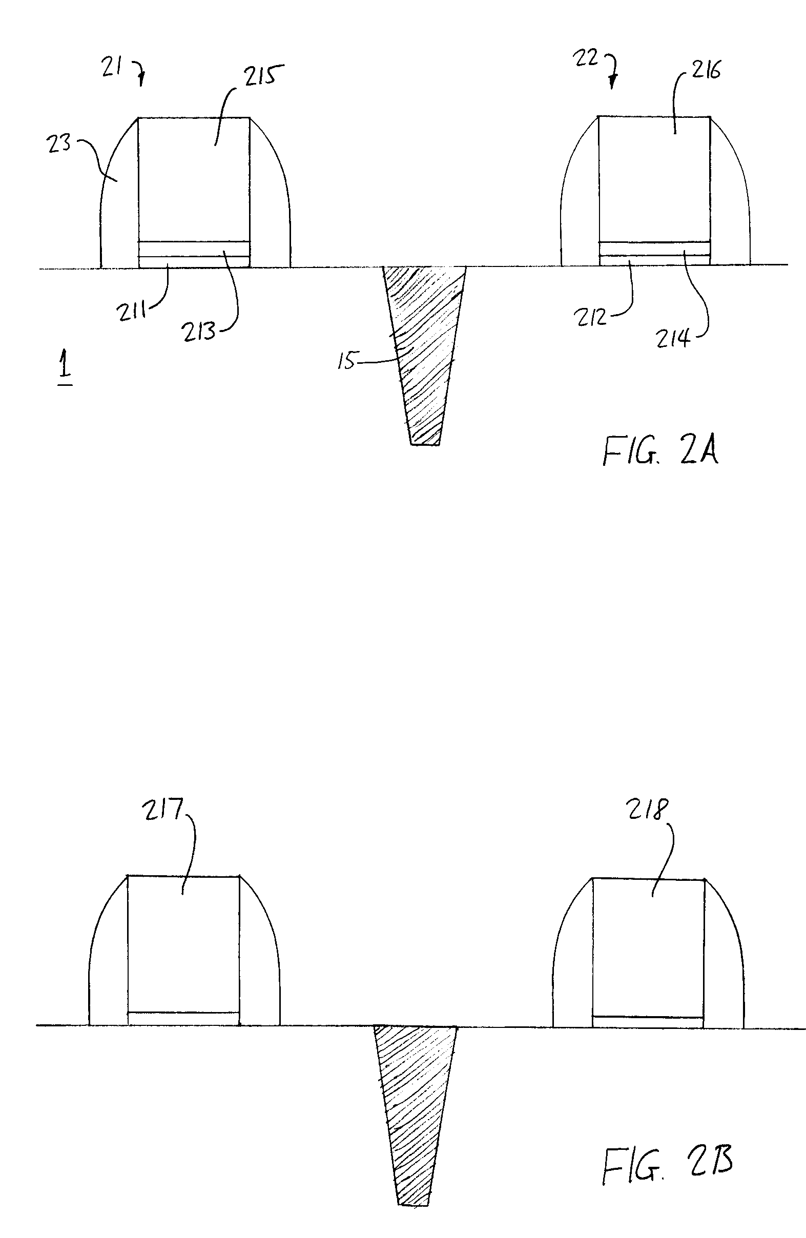
[0031]FIGS. 2A and 2B are schematic illustrations of CMOS gate structures fabricated in accordance with the present invention. NFET and PFET devices are typically fabricated in pairs, while being electrically isolated from each other. This is illustrated in FIG. 2A and subsequent figures by NFET gate 21, PFET gate 22 (each having a gate stack, a gate dielectric, and spacers 23) and trench isolation 15 between them. Other details of the NFET and PFET devices (such as the source and drain regions formed in substrate 1) are omitted for the sake of clarity.

[0032] Each of the gate structures 21, 22 in FIG. 2A has a refractory metal nitride layer 213, 214 in contact with the gate dielectric 211, 212 in the NFET and PFET devices respectively. The refractory metal nitride layer is generally MNx, where M indicates a metal such as W, Re, Zr, or Hf, and x indicates the proportion of nitrogen in the nitride. A preferred material is tungsten nitride, WN...


PUM

PropertyMeasurementUnit
temperaturesaaaaaaaaaa
thicknessaaaaaaaaaa
equivalent oxide thicknessaaaaaaaaaa

Abstract

An integrated circuit is provided including an FET gate structure formed on a substrate. This structure includes a gate dielectric on the substrate, and a metal nitride layer overlying the gate dielectric and in contact therewith. This metal nitride layer is characterized as MNx, where M is one of W, Re, Zr, and Hf, and x is in the range of about 0.7 to about 1.5. Preferably the layer is of WNx, and x is about 0.9. Varying the nitrogen concentration in the nitride layer permits integration of different FET characteristics on the same chip. In particular, varying x in the WNx layer permits adjustment of the threshold voltage in the different FETs. The polysilicon depletion effect is substantially reduced, and the gate structure can be made thermally stable up to about 1000° C.

Description

BACKGROUND OF INVENTION [0001] This application is related to Application No. FIS9-2003-0417-US1, “High temperature stable gate structure with metallic electrode,” filed the same day and assigned to the same assignee as the present application. The disclosure of the related application is incorporated herein by reference. [0002] This invention relates to the manufacture of advanced semiconductor devices, particularly complementary metal-oxide-semiconductor (CMOS) FET devices, including p-type and n-type FETs (PFETs and NFETs respectively). More particularly, the invention relates to fabrication of gate structures for these devices having stable electrical and chemical characteristics at temperatures up to 1000° C. [0003] The ongoing reduction in size of electronic device elements poses problems in device performance which must be addressed using new materials and fabrication techniques. In the case of gate structures for high-performance CMOS devices, the equivalent oxide thickness ...

Claims


Application Information

Patent Timeline
Patent Type & Authority Applications(United States)
IPC IPC(8): H01L21/8238H01L29/76
CPCH01L21/823842Y10S438/942Y10S257/90H01L21/823857
Inventor PARK, DAE-GYUCABRAL, CYRIL JR.GLUSCHENKOV, OLEGKIM, HYUNGJUN
Owner GLOBALFOUNDRIES US INC
Why Eureka
Try Eureka