Semiconductor element and display device using the same

Inactive Publication Date: 2005-12-22
SEMICON ENERGY LAB CO LTD
View PDF99 Cites 45 Cited by
  • Summary
  • Abstract
  • Description
  • Claims
  • Application Information

AI Technical Summary

Benefits of technology

[0033] As described above, when the thin film transistor using the organic resin film as the interlayer insulating film is manufactured, the photosensitive organic resin film is used as the interlayer insulating film and the contact structure shown in FIGS. 1A and 1B is employed. Thus, the thin f

Problems solved by technology

The circuits composed of the thin film tr

Method used


Image

  • Semiconductor element and display device using the same
  • Semiconductor element and display device using the same
  • Semiconductor element and display device using the same

Examples


embodiment 1

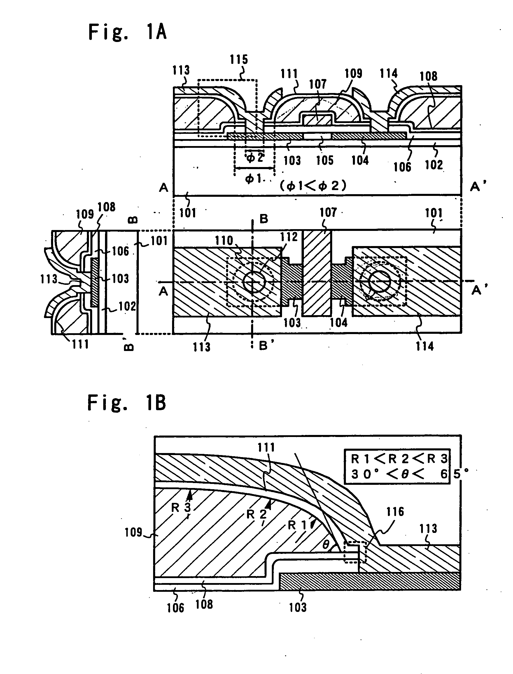
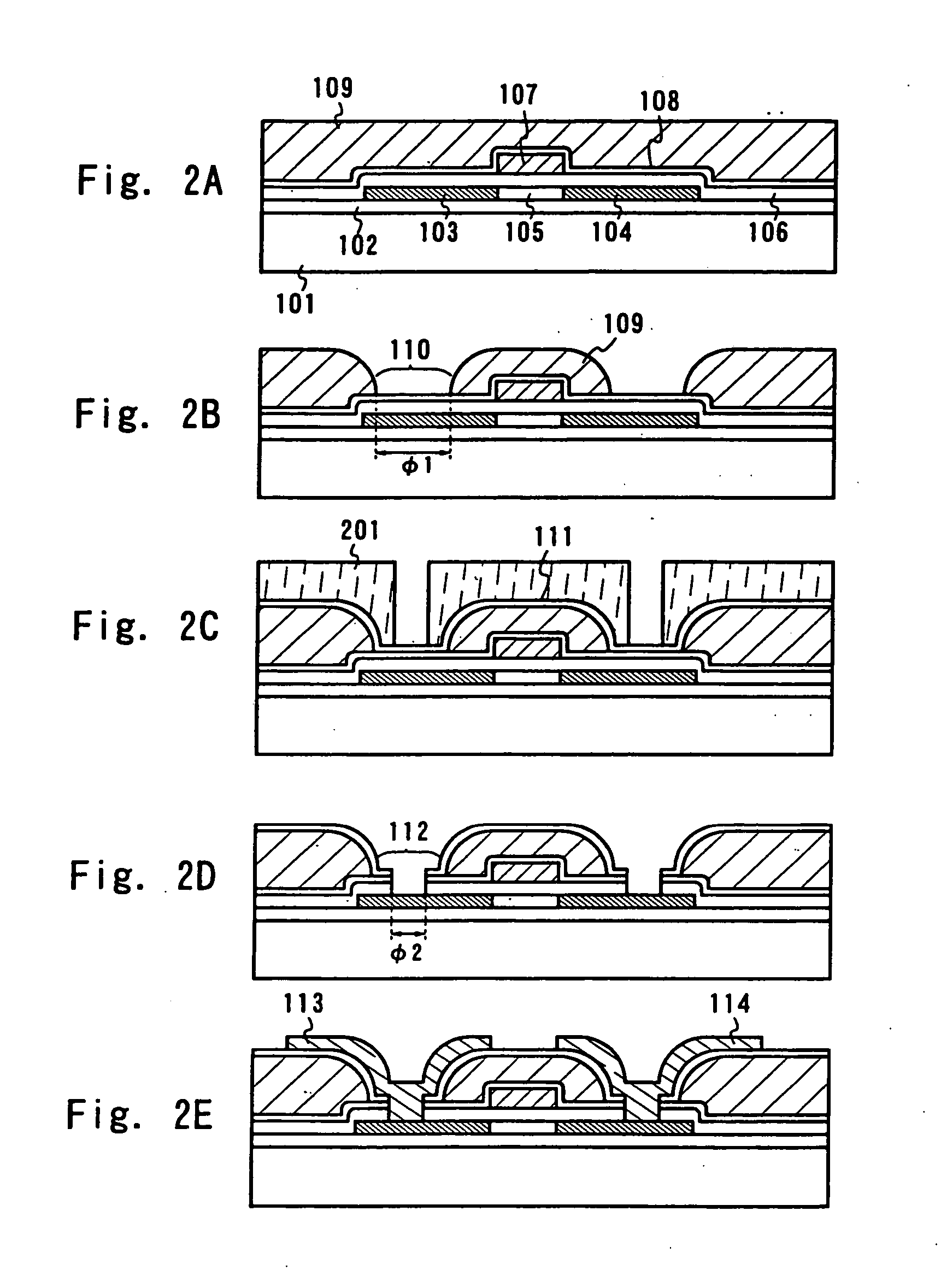
[0052] In this embodiment, an example in which the formation position of the first opening portion 110 is changed in FIGS. 1A and 1B will be described using FIGS. 8A and 8B. Note that FIGS. 8A and 8B each show a cross sectional structure immediately after the formation of the second opening portion. In addition, the reference symbols used in FIGS. 1A and 1B are referred to if necessary.

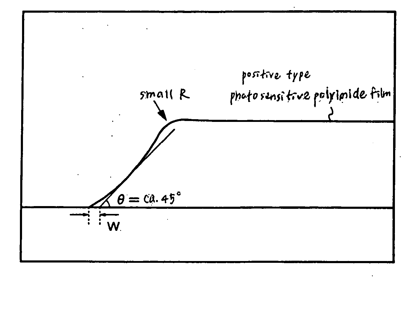
[0053] In FIG. 8A, reference numeral 801 denotes a first opening portion having a diameter of φ1 and 802 denotes a second opening portion having a diameter of φ2. A characteristic in FIG. 8A is that the first opening portion 801 is provided to protrude from the end portion of the source region 103. The photosensitive organic resin film 109 can be formed in a position as indicated in this embodiment because the first passivation film 108 becomes an etching stopper, thereby stopping the progress of etching. In addition, in FIG. 8B, reference numeral 803 denotes a first opening portion having a diameter...

embodiment 2

[0055] In this embodiment, an example in which the present invention is applied to a light emitting device such as an EL display device will be described. FIG. 9A is a plan view of a pixel of the light emitting element (note that a state up to the formation of a pixel electrode is indicated), FIG. 9B is a circuit diagram thereof, and FIGS. 9C and 9D each are a cross sectional view along a line A-A′ or B-B′.

[0056] As shown in FIGS. 9A and 9B, a display portion of the light emitting device includes a plurality of pixels which are surrounded by gate wirings 951, data wirings 952, and power source wirings (wirings for supplying a constant voltage or a constant current) 953 and arranged in matrix. In each of the pixels, a TFT 954 serving as a switching element (hereinafter referred to as a switching TFT), a TFT 955 serving as means for supplying a current or a voltage for producing light emission of an EL element (hereinafter referred to as a driver TWT), a capacitor portion 956, and an...

embodiment 3

[0077] In this embodiment, an example is indicated in which a connection structure between the drain wiring 921 and the pixel electrode 958 is modified in the light emitting device described in Embodiment 2. Note that the fundamental structure is not changed as compared with that shown in FIG. 9C. Thus, in this embodiment, reference symbols are provided to only necessary portions and the description will be made.

[0078] As shown in FIG. 11A, a pixel electrode 501 made from an oxide conductive film is formed and then a drain wiring 502 is formed, so that a structure in which the drain wiring 502 is in contact with the pixel electrode 501 so as to cover the end portion thereof is obtained. When such a structure is obtained, the pixel electrode 501 may be formed after the formation of a second opening portion 503. Alternatively, the second opening portion 503 may be formed after the formation of the pixel electrode 501. In any case, even when dry etching processing is conducted, the ph...


PUM


Abstract

Provided is a semiconductor element including: a semiconductor having an active layer; a gate insulating film which is in contact with the semiconductor; a gate electrode opposite to the active layer through the gate insulating film; a first nitride insulating film formed over the active layer; a photosensitive organic resin film formed on the first nitride insulating film; a second nitride insulating film formed on the photosensitive organic resin film; and a wiring provided on the second nitride insulating film, in which a first opening portion is provided in the photosensitive organic resin film, an inner wall surface of the first opening portion is covered with the second nitride insulating film, a second opening portion is provided in a laminate including the gate insulating film, the first nitride insulating film, and the second nitride insulating film inside the first opening portion, and the semiconductor is connected with the wiring through the first opening portion and the second opening portion.

Description

BACKGROUND OF THE INVENTION [0001] 1. Field of the Invention [0002] The present invention relates to a semiconductor element (typically, a transistor) and a manufacturing method thereof, and more specifically belongs to a technique of a display device using a thin film transistor as a device. That is, the present invention belongs to a technique concerning a display device represented by a liquid crystal display device, an electroluminescence display device, or the like, a technique concerning a sensor represented by a CMOS sensor or the like, and other techniques concerning various semiconductor devices in which a semiconductor integrated circuit is mounted. [0003] 2. Description of the Related Art [0004] In recent years, the developments for a liquid crystal display device and an electroluminescence display device in which thin film transistors (TFTs) are integrated on a glass substrate have been progressed. These display devices each are one of semiconductor devices characterized...

Claims


Application Information

Patent Timeline
IPC IPC(8): G02F1/1362H01L21/336H01L27/32
CPCG02F1/136227H01L27/3248H01L29/66757H01L29/66765H01L2251/5315H01L27/124Y10S438/95H01L2924/0002H01L29/78606H01L23/49827H01L2924/00H10K59/123H10K2102/3026H01L27/1248H01L29/786H01L23/3171H01L29/41733H01L29/42384H10K59/124H10K59/131H10K2102/311H01L29/78651G02F1/133512G02F1/1337G02F1/1339G02F1/1341G02F1/13439G02F1/136213G02F1/136286G02F1/1368G02F2201/123H01L27/1218
Inventor MURAKAMI, SATOSHIHAYAKAWA, MASAHIKOYAMAZAKI, SHUNPEI
Owner SEMICON ENERGY LAB CO LTD
Why Eureka
Try Eureka