Sequential station tool for wet processing of semiconductor wafers

a technology of semiconductor wafers and station tools, applied in the field of sequential wet processing of silicon wafers, can solve the problems of difficult maintenance of batch uniformity, difficult balance of software logic, and critical issues in wafer throughput and wafer uniformity, so as to improve wafer throughput, process and hardware flexibility, and reproducibility of wafer to wafer

Inactive Publication Date: 2005-12-22
NOVELLUS SYSTEMS
View PDF16 Cites 42 Cited by
  • Summary
  • Abstract
  • Description
  • Claims
  • Application Information

AI Technical Summary

Benefits of technology

[0009] The present invention provides methods and apparatus for processing semiconductor wafers sequentially. More particularly this invention provides impr...

Problems solved by technology

In integrated circuit fabrication, wafer throughput and wafer uniformity are critical issues.
Batch uniformity can be difficult to maintain under such scenarios, given the multitude of factors necessary to control and reproduce, as well as the tight analytical control of plating bath composition associated with integrated circuit fabrication.
For these systems, although multiple wafers are processed simultaneously, individual plating and post-plating operations (unit operations) do not generally require the same processing time frames, often robotics handling events and software logic are difficult to balance and wafer throughput is hard to fully optimize.
In a conven...

Method used


Image

  • Sequential station tool for wet processing of semiconductor wafers
  • Sequential station tool for wet processing of semiconductor wafers
  • Sequential station tool for wet processing of semiconductor wafers

Examples


Embodiment Construction

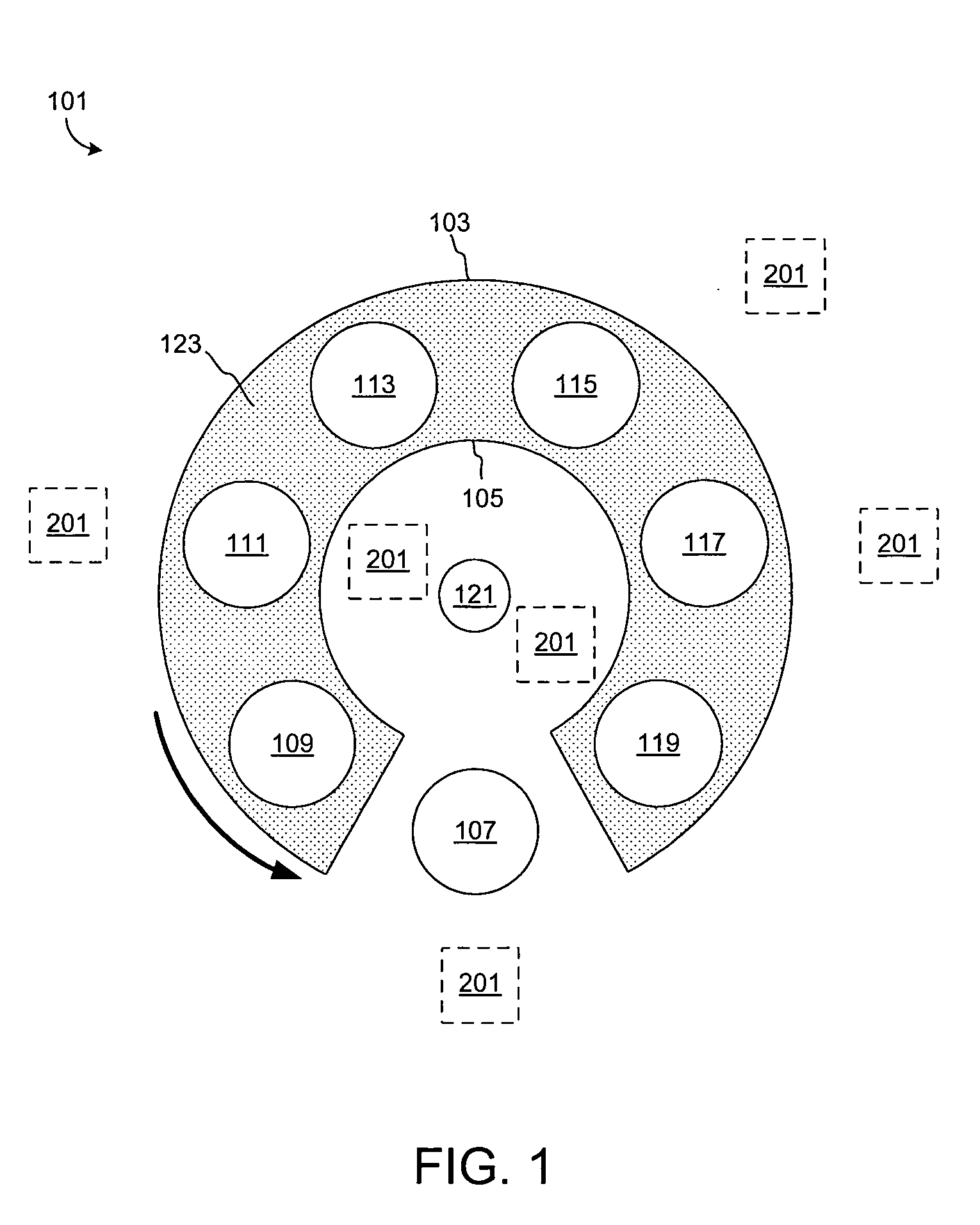
[0023] In the following detailed description of the present invention, numerous specific embodiments are set forth in order to provide a thorough understanding of the invention. However, as will be apparent to those skilled in the art, the present invention may be practiced without these specific details or by using alternate elements or processes. For example, one aspect of the apparatus of the invention is depicted as a radial (carousel) arrangement; this aspect of the invention could be embodied in a linear (straight track) arrangement, or some combination or variation of either arrangement. In some descriptions herein, well-known processes, procedures, and components have not been described in detail so as not to unnecessarily obscure aspects of the present invention.

[0024] One method of the invention features electroplating a metal such as copper on a semiconductor wafer by sequentially exposing the wafer to distinct sub-processes of the overall electroplating process. These a...


PUM

PropertyMeasurementUnit
Compositionaaaaaaaaaa
Aspect ratioaaaaaaaaaa

Abstract

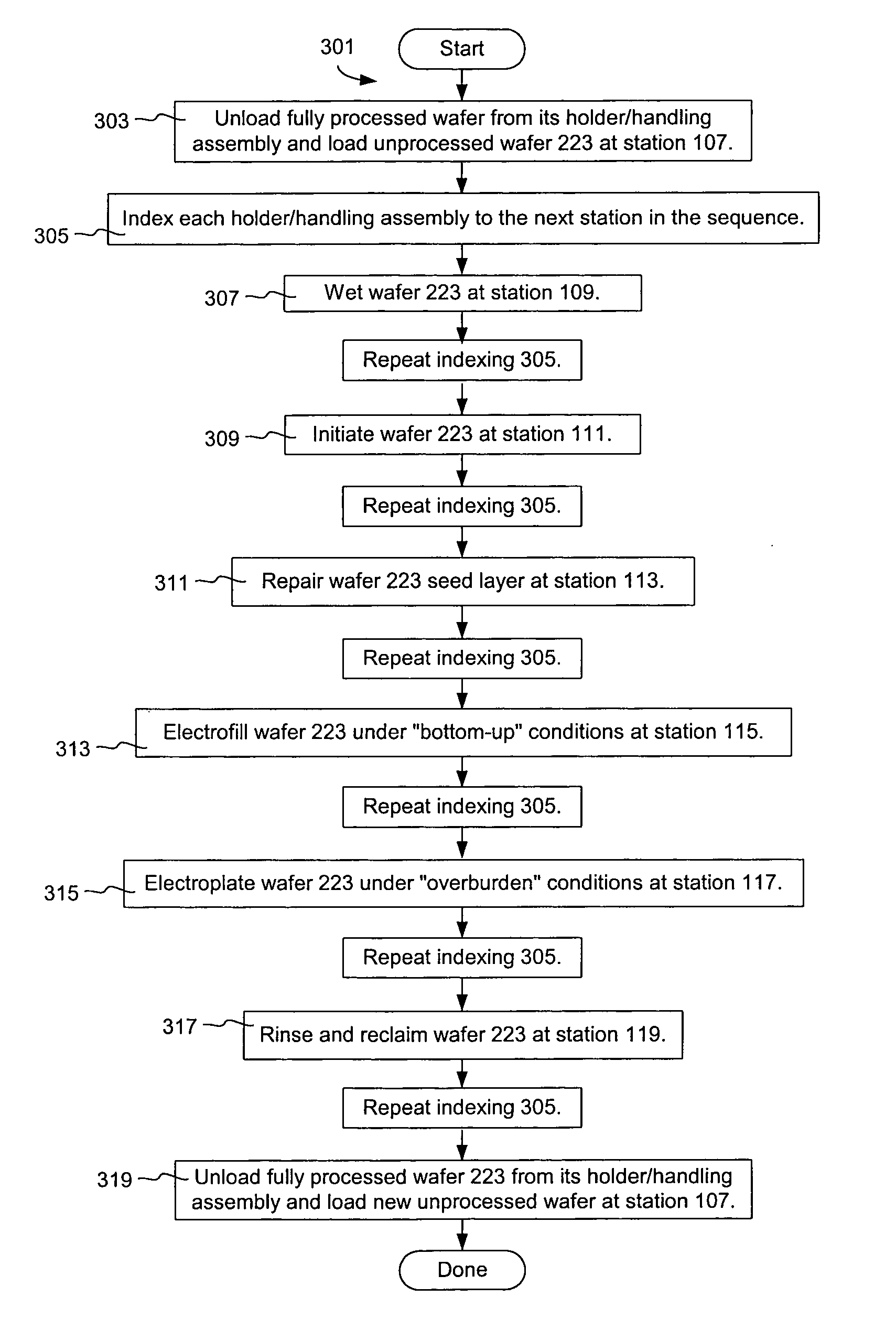
Methods and apparatus are provided for processing semiconductor wafers sequentially. Sequential processes employ multi-station processing modules, where particular encompassing wafer processes are divided into sub-processes, each optimized for increasing wafer to wafer uniformity, result quality, and overall wafer throughput. In one example, a copper electroplating module includes separate stations for wetting, initiation, seed layer repair, fill, overburden, reclaim, and rinse.

Description

CROSS-REFERENCE TO RELATED APPLICATIONS [0001] This application is a continuation, claiming priority under 35 U.S.C. § 120, from U.S. patent application Ser. No. 09 / 828,371, filed Apr. 5, 2001 naming Patton et al., and titled “SEQUENTIAL STATION TOOL FOR WET PROCESSING OF SEMICONDUCTOR WAFERS.” That application is incorporated herein by reference for all purposes.FIELD OF THE INVENTION [0002] This invention relates to semiconductor wafer processing technology. More specifically, it relates to processing of partially fabricated integrated circuits. Even more specifically, the invention pertains to particular methods and apparatus for sequential wet processing of silicon wafers in integrated circuit fabrication. BACKGROUND OF THE INVENTION [0003] In integrated circuit fabrication, wafer throughput and wafer uniformity are critical issues. Wafer wet processes such as, for example electroplating, require precise conditions i.e. anode configuration, field shape, electrolyte composition, ...

Claims


Application Information

Patent Timeline
IPC IPC(8): C25D3/38C25D5/10H01L21/00H01L21/288H01L21/44H01L21/677
CPCC25D3/38C25D5/10H01L21/2885H01L21/67161Y10T29/41H01L21/6723H01L21/67751C25D17/001H01L21/76877H01L21/6719
Inventor PATTON, EVAN E.CACOURIS, THEODOREBROADBENT, ELIOTMAYER, STEVEN T.
Owner NOVELLUS SYSTEMS
Why Eureka
Try Eureka