Supercharge Your Innovation With Domain-Expert AI Agents!

Method and apparatus for the improvement of material/voltage contrast

a voltage contrast and material technology, applied in the direction of individual semiconductor device testing, semiconductor/solid-state device testing/measurement, instruments, etc., can solve the problems of limited access to the lower metal layer from the wafer frontside, introduction of operational complexity, and ineffective prior methods for imaging non-biased regions. , to achieve the effect of enhancing voltage contrast and high quality

Inactive Publication Date: 2006-01-12
ROY ERWAN LE
View PDF0 Cites 6 Cited by
  • Summary
  • Abstract
  • Description
  • Claims
  • Application Information

AI Technical Summary

Benefits of technology

Enables precise registration of CAD to FIB images and accurate endpointing during trench milling, facilitating non-destructive and accurate editing of ICs without optical imaging or voltage biasing, while also enabling imaging of vertical doping profiles.

Problems solved by technology

The stacking of increasingly large numbers of metal layers has limited the access to lower metal layers from the wafer frontside.
In addition, the widespread use of flipchip mounting, wherein the IC is mounted face down on a packaging substrate, leaving only the backside of the chip exposed, precludes front side access to the chip.
A challenge in backside editing is navigation, i.e., locating the exact circuit node where a modification or repair is needed.
However, this prior method is not effective in imaging non-biased regions.
Additionally, operational complexity is introduced by this method, since a special socket for each particular device and the interconnect board to the electrical bias is required to provide the bias, and an increased knowledge level is required to know which pins should be biased relative to which others.

Method used


Image

  • Method and apparatus for the improvement of material/voltage contrast
  • Method and apparatus for the improvement of material/voltage contrast
  • Method and apparatus for the improvement of material/voltage contrast

Examples


Embodiment Construction

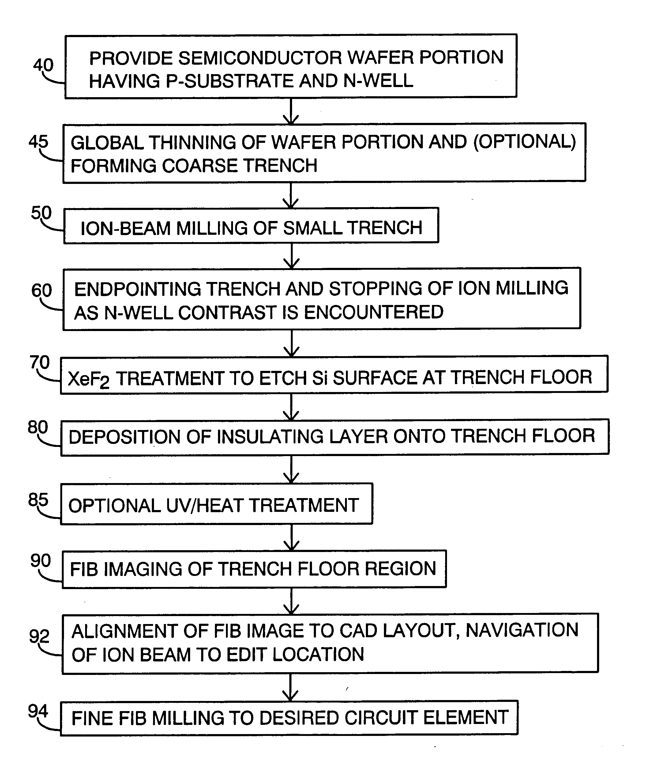
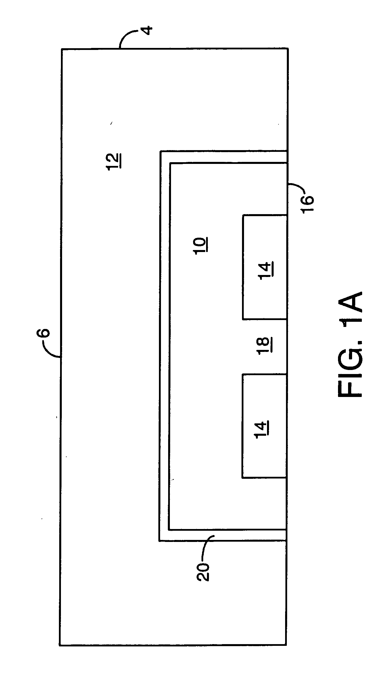
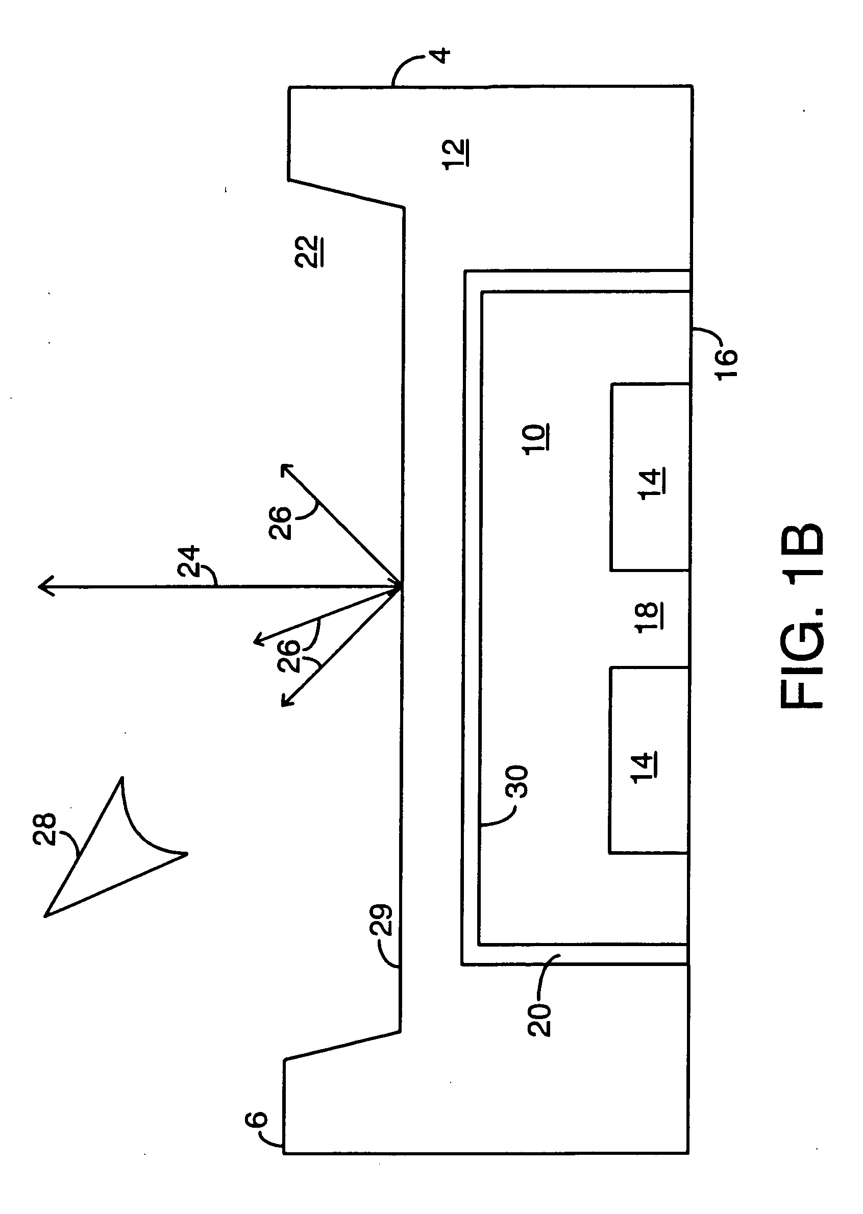
[0034] The present invention provides a method and a system for implementing the method, for inducing steady state voltage contrast between regions on an IC chip backside, so as to observe structures on a FIB image. The inventive method enables the FIB imaging without necessity of external voltage bias of the n-well regions. It further enables the use of the FIB ion beam to map the wafer from the backside, i.e., to locate positions of various materials and diffusion regions. The method is believed to be based on differential capacitive characteristics of an MOS-like structure (M=Induced Surface Conductive layer created by the beam interaction with an oxide; O=oxide; S=underlying semiconductor) which affect the secondary electron emission from the substrate. The surface of the exposed wafer backside acts as the top plate of a capacitor, a layer or feature below the surface acts as the bottom plate of the capacitor, and the intervening material or materials such as silicon or silicon ...


PUM

PropertyMeasurementUnit
beam currentaaaaaaaaaa
timeaaaaaaaaaa

Abstract

A method and system for registering a CAD layout to a Focused Ion Beam image for through-the substrate probing, without using an optical image and without requiring biasing, includes an improved method of trench endpointing during the FIB milling operation with a low beam energy. The method further includes removal of Ga at the trench floor using XeF2, as well as the deposition of an insulating layer onto the trench floor.

Description

CROSS REFERENCE TO RELATED APPLICATIONS [0001] This application is a divisional of copending U.S. application Ser. No. 10 / 789,336, filed on Feb. 27, 2004, and claims priority thereto. The specification of U.S. application Ser. No. 10 / 789,336 is hereby incorporated by reference. [0002] This application is further related to U.S. Provisional Applications No. 60 / 450,636 by Erwan Le Roy and William Thompson, filed Feb. 28, 2003, and No. 60 / 523,063 by Erwan Le Roy and William Thompson, filed Nov. 18, 2003, and claims priority to both of these provisional applications. [0003] This application is further related to commonly owned U.S. application Ser. No. 10 / 758,146 entitled “METHOD AND SYSTEM FOR INTEGRATED CIRCUIT BACKSIDE NAVIGATION”, filed Jan. 14, 2004.BACKGROUND OF THE INVENTION [0004] As IC technology advances and device dimensions decrease while circuit speeds increase, packaging and diagnostic techniques have advanced accordingly. Methods for modification and editing of circuits a...

Claims


Application Information

Patent Timeline
Patent Type & Authority Applications(United States)
IPC IPC(8): G01R31/26H01J37/305H01L21/316H01L21/66
CPCG01N23/2251Y10T29/41H01J37/3005H01J37/3056H01J2237/30466H01J2237/3174H01J2237/31749H01L21/02164H01L21/02214H01L21/02348H01L21/31608H01L22/12H01L22/26H01L22/34H01L2924/0002G01R31/307H01L2924/00
Inventor ROY, ERWAN LE
Owner ROY ERWAN LE
Features
  • R&D
  • Intellectual Property
  • Life Sciences
  • Materials
  • Tech Scout
  • Unparalleled Data Quality
  • Higher Quality Content
  • 60% Fewer Hallucinations
Learn More