Modular tool unit for processing microelectronic workpieces

a technology of microelectronic workpieces and tool units, applied in the direction of basic electric elements, semiconductor/solid-state device manufacturing, electric apparatus, etc., can solve the problems of device failure, device open or short circuit condition, device polish rate affecting the ultimate uniformity of the surface of the polished copper structure, etc., to improve the efficiency of manufacturing custom integrated tool assemblies

Inactive Publication Date: 2006-01-12
SEMITOOL INC
View PDF15 Cites 20 Cited by
  • Summary
  • Abstract
  • Description
  • Claims
  • Application Information

AI Technical Summary

Benefits of technology

[0017] One aspect of the present invention is directed toward a modular thermal processing unit that can be a stand-alone unit that operates by itself, or connected to one or more modular tool units to customize the configuration of a modular tool system. The modular thermal processing unit has a dimensionally stable mounting module that enables individual modular tool units to be connected together in a manner that maintains relative positions between individual components and a transport system in a fixed reference frame defined by the mounting module. One benefit of the modular thermal processing unit of the present invention is that it can be connected with other modular tool units to produce different tool configurations. Accordingly, tool manufacturers can use a universal modular tool unit to produce different tools with different configurations of processing stations in a manner that enhances the efficiency of manufacturing custom integrated tool assemblies.

Problems solved by technology

Wafer-to-wafer and within wafer grain size variability in the copper film can adversely affect the polish rate of the chemical mechanical processing as well as the ultimate uniformity of the surfaces of the polished copper structures.
Such devices may fail if the copper metallization exhibits excessive electromigration that ultimately results in an open or short circuit condition in one or more of the metallization features.
These batch process units increase throughput time and are not easily integrated with existing processing equipment.
One potential drawback with this device is that the chamber encloses a large volume which can be expensive and time consuming to fill with purge gas and / or process gas.
Another potential drawback is that the heater may not efficiently transfer heat to the heat plate.
Still a further drawback is that the heater plate may continue to heat the wafer after the heating phase of the annealing process is complete, and may limit the efficiency of the cold plate.
Accordingly, the device may be inadequate and / or too time consuming for use in an annealing process because the wafer must be placed in the heating chamber, then removed from the heating chamber and placed in the cooling chamber for each annealing cycle.
Furthermore, the transfer arm that moves the wafer from one chamber to the next will generally not have the same temperature as the wafer when it contacts the wafer, creating a temperature gradient on the wafer that can adversely affect the uniformity of sensitive thermal processes.
None of the prior batch or single wafer annealing assemblies have been integrated into a modular system for continuous processing of workpieces to improve overall manufacturing efficiencies.
Although the process of manually aligning the components of the robot to the reference frame and manually teaching the robot the location of each component in the tool is an accepted method for setting up a tool, it is also out of specifications sooner, which results in taking the tool offline more frequently.
Therefore, the downtime associated with calibrating the transport system and repairing / maintaining electrochemical deposition chambers significantly impacts the costs of operating wet chemical processing tools.
Another challenge of integrating independent processing tools into a system is cost-effectively manufacturing and installing the tools to meet demanding customer specifications.
It is expensive and inefficient to manufacture a large number of different platform configurations to meet the needs of the individual customers.

Method used


Image

  • Modular tool unit for processing microelectronic workpieces
  • Modular tool unit for processing microelectronic workpieces
  • Modular tool unit for processing microelectronic workpieces

Examples


Embodiment Construction

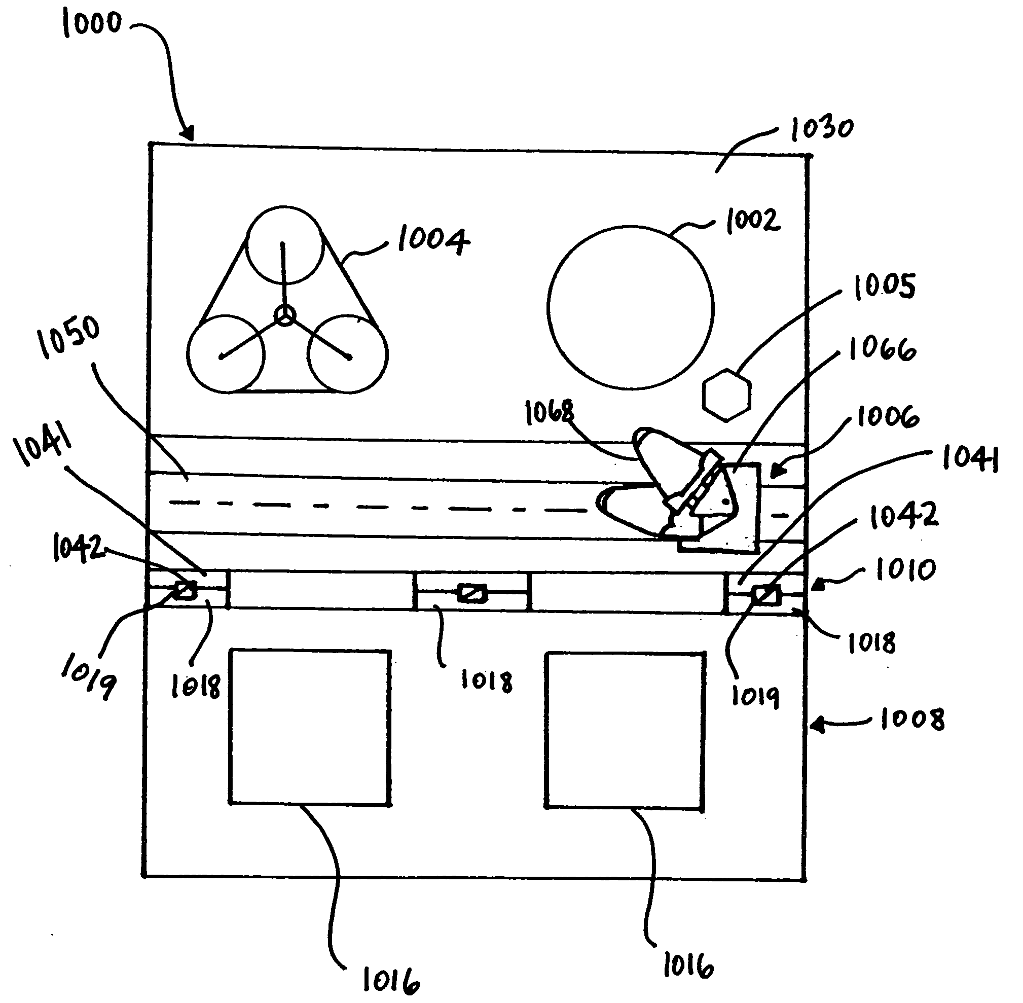
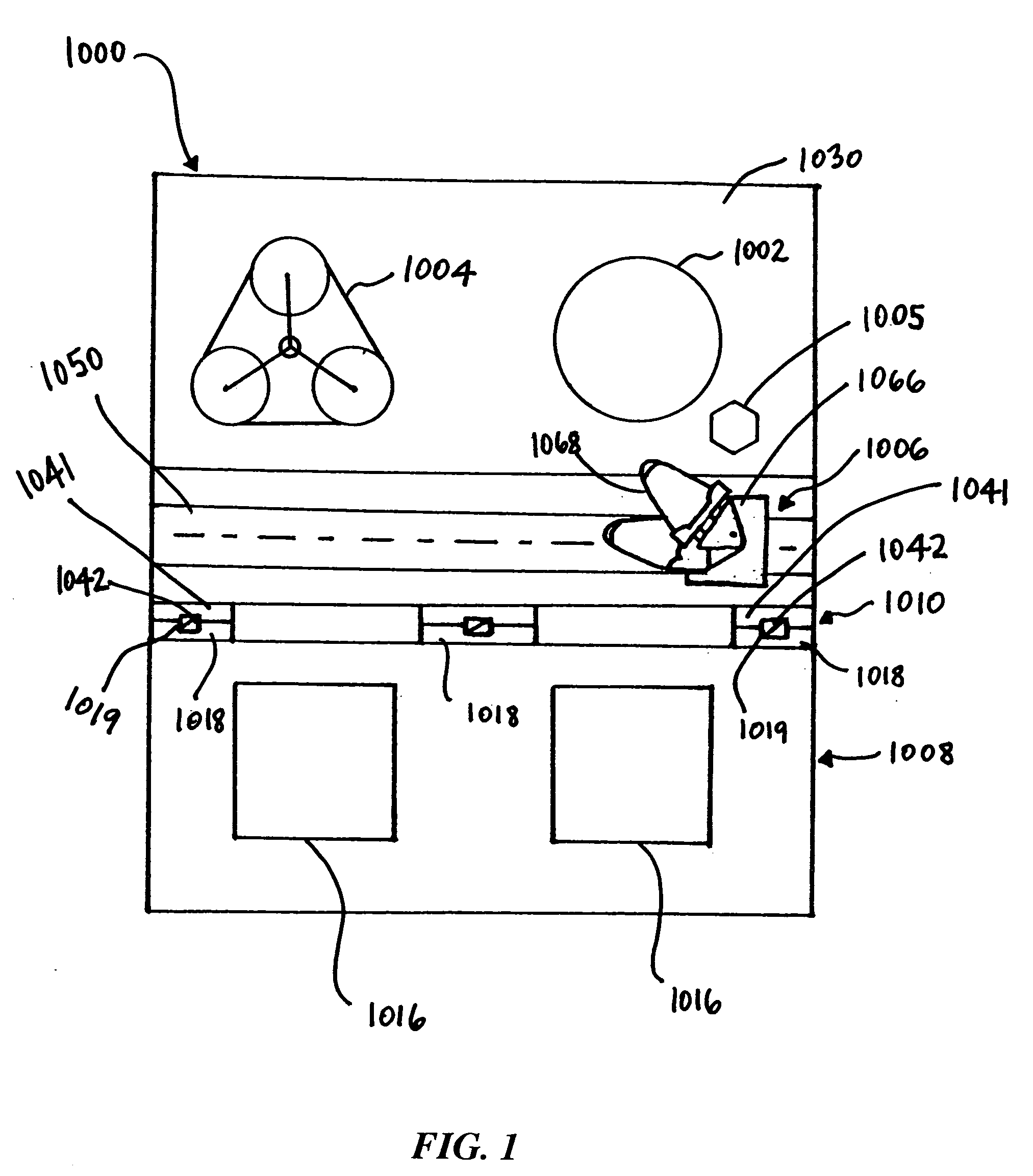
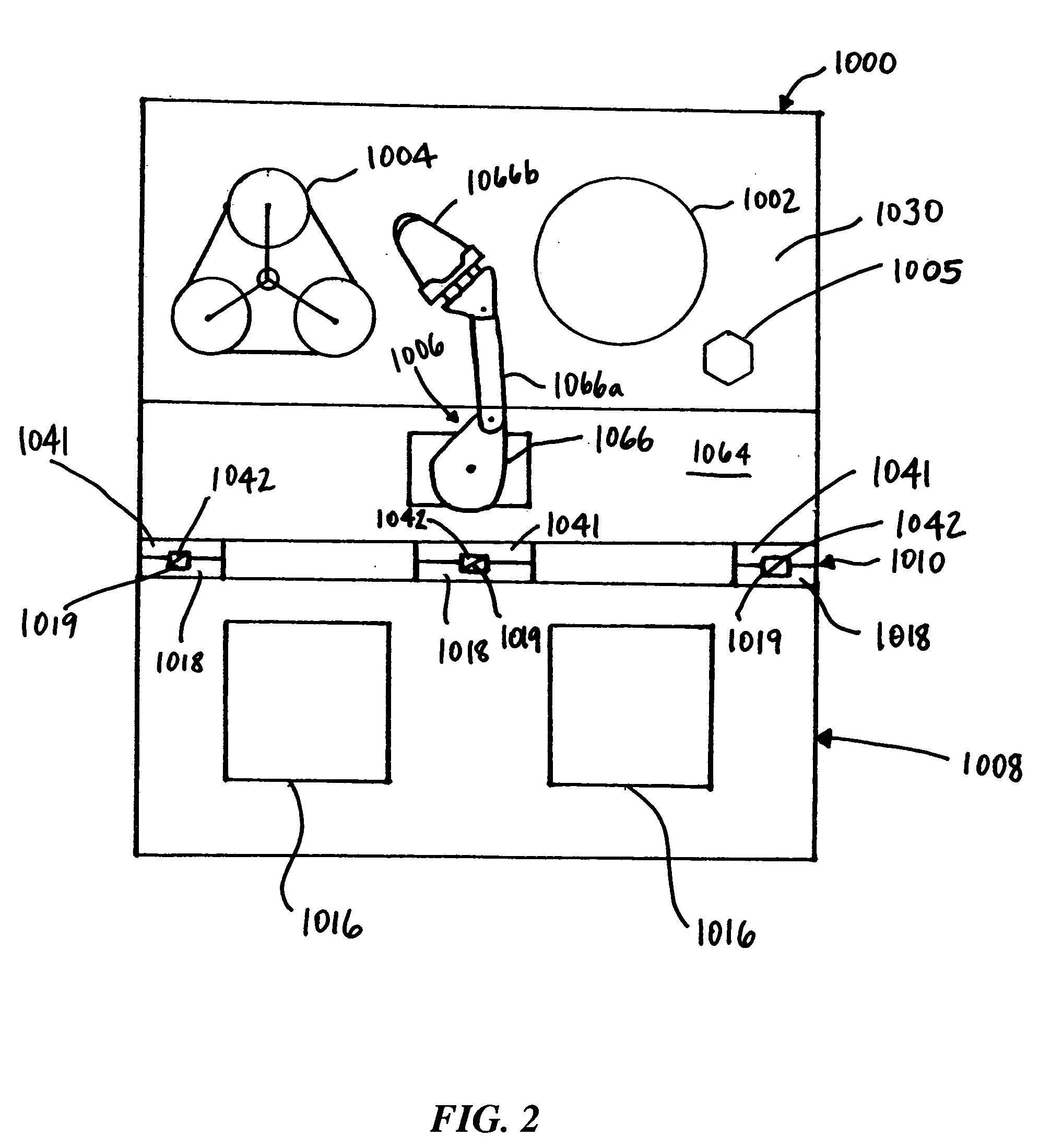
[0061] For purposes of the present application, a microelectronic workpiece is defined to include a workpiece formed from a substrate upon which microelectronic circuits or components, data storage elements or layers, and / or micromechanical elements are formed. Micromachines or micromechanical devices are included within this definition because they are manufactured using much of the same technology that is used in the fabrication of integrated circuits. The workpieces can be semiconductive pieces (e.g., doped silicon wafers or gallium arsenide wafers), dielectric pieces (e.g., various ceramic substrates) or conductive pieces. Although the present invention is applicable to this wide range of products, the invention will be particularly described in connection with its use in the production of interconnect structures formed during the production of integrated circuits on a semiconductor wafer.

[0062] Various embodiments of intermediate mounting modules and modular tool units for the...


PUM


Abstract

A modular apparatus for thermally processing a microelectronic workpiece is provided. The modular apparatus comprises a mounting module having a rotatable carousel assembly configured to support at least one workpiece. A driver is coupled to the carousel assembly and rotates the carousel assembly, moving the workpiece between a loading station, a heating station and a cooling station. The thermal processing modular apparatus has a front docking unit for removeably connecting it to a load/unload module and a rear docking unit for removeably connecting it to a wet chemical processing tool, or another tool for otherwise processing a workpiece. A transport system (i.e., robot) services the modular tool units that can be automatically calibrated to work with individual processing components of the tool units.

Description

CROSS-REFERENCE TO RELATED APPLICATIONS [0001] This application is a continuation-in-part of U.S. patent application Ser. No. 10 / 987,049, filed Nov. 12, 2004, now pending; and claims priority from provisional U.S. Patent Application No. 60 / 586,833, filed Jul. 9, 2004, and provisional U.S. Patent Application No. 60 / 586,981, filed Jul. 9, 2004. Priority to these applications is claimed under 35 U.S.C. §§ 119 and 120, and the disclosure of these applications is incorporated herein by reference in their entirety.FEDERALLY SPONSORED RESEARCH OR DEVELOPMENT [0002] Not applicable. TECHNICAL FIELD [0003] The present invention is directed toward apparatus and methods for processing microfeature workpieces having a plurality of microdevices integrated in and / or on the workpieces. Particular aspects of the invention relate to a modular tool unit for heat treating microelectronic workpieces that can be combined with other processing units (e.g., wet chemical processing tools) to customize workp...

Claims


Application Information

Patent Timeline
Patent Type & Authority Applications(United States)
IPC IPC(8): H01L21/00
CPCH01L21/67098H01L21/67775H01L21/67196H01L21/67173
Inventor WIRTH, PAUL ZACHARYDAVIS, JEFFRY ALANHARRIS, RANDY A.
Owner SEMITOOL INC
Why Eureka
Try Eureka