Image forming method, image forming apparatus and process cartridge therefor

a technology of image forming apparatus and process cartridge, which is applied in the direction of electrographic process apparatus, corona discharge, instruments, etc., can solve the problems of insufficient photographic image production, insufficient development of ultra high-resolution electrophotographic image forming apparatus, etc., and achieve high durability, high resolution, and stably producing high-quality images.

Inactive Publication Date: 2006-01-19
RICOH KK
View PDF29 Cites 32 Cited by
  • Summary
  • Abstract
  • Description
  • Claims
  • Application Information

AI Technical Summary

Benefits of technology

[0043] Accordingly, an object of the present invention is to provide an image forming method and an image forming apparatus using an electrophotographic photoreceptor capable of forming images having an ultra high resolution not less than 1,200 dpi and up to 2,400 dpi, and stably producing high-quality images with high durability.
[0044] Another object of the present invention is to provide an image forming method using a photoreceptor having stable electrical properties, wherein the abrasion of a photosensitive layer thereof due to repeated image formation for long periods is inhibited.
[0045] A further object of the present invention is to provide an image forming method wherein defective images such as blurred images, toner filming and black spots due to repeated image formation for long periods are inhibited.

Problems solved by technology

The current electrophotographic image forming apparatus has an image resolution of from 300 to 600 dpi, which is insufficient to produce photographic images.
However, an ultra high-resolution electrophotographic image forming apparatus satisfying all these is not developed yet.
However, just a small beam spot diameter could not produce ultra high resolution images.
When the conventional multilayer photoreceptor is used, light having a very short wavelength is absorbed in a charge transport layer thereof, resulting in low sensitivity of the photoreceptor.
Even when the light having a small beam diameter is irradiated to a charge generation layer of an electrophotographic photoreceptor, it is still difficult therefor to produce ultra high resolution images.
However, when the photosensitive layer is thin, deterioration of the charge stability, life and dot reproducibility due to concavities and convexities of the electroconductive substrate tend to occur.
A photosensitive layer having a pin hole or a coating defect causing a dielectric breakdown occasionally causes production of defective images.
However, the single-layered photoreceptor has less sensitivity and more residual potential than the multilayer photoreceptor, and still has a problem when used for a high-speed electrophotographic image forming apparatus.
However, since the fragile and thin charge generation layer formed as an outermost layer receives mechanical and chemical stress from a charger, image developer, a transferer and a cleaner, the photoreceptor noticeably deteriorates due to repeated use and is practicable.
However, the purpose thereof is to provide an electrophotographic image forming apparatus producing less ozone to reduce environmental burdens, and which is not designed for an ultra high resolution electrophotographic image forming apparatus.
When the formation of a latent image is impaired, high quality images without contamination cannot be produced.
Furthermore, the recent contact or non-contact chargers, being located quite closer to the surface of the photoreceptor and corona discharging than a conventional charger, damages the photoreceptor more and cuts molecular chains of constituents in the surface thereof.
However, even the photoreceptor using a BPZ polycarbonate binder has insufficient abrasion resistance and does not have sufficient durability.
On the other hand, although the photoreceptor including the hardening silicone resin including a colloidal silica in its surface layer improves the abrasion resistance thereof, the photoreceptor tends to produce foggy or blurred images when repeatedly used and has insufficient durability.
Therefore, a moisture absorbed therein in an environment of high temperature and high humidity can not be removed, resulting in occurrence of paper dust and toner filming, and production of defective images such as blurred, striped or spotted images.
However, the surface protective layer including an organic or inorganic filler occasionally scatters laser beam therein when irradiated therewith to disturb a laser spot.
In addition, a coating liquid including the filler is difficult to disperse, which causes problems of the surface protective layer.
Particularly, a hard inorganic filler causes a microscopic nonuniformity such as hard projections thereon, resulting in chipping blade and toner filming.
As mentioned above, although the organic photoreceptor has a disadvantage of being abraded with a mechanical load from an image developer and a cleaner, the cleaner is forced to have a harder cleaning rubber blade and higher contact pressure to remove a toner having a smaller particle diameter for higher image quality.
A damage due to a local abrasion causes defective cleaning, resulting in production of striped images.
(1) The crosslinked charge transport layer including a hardening binder tends to increase residual potential and deteriorate image density because of poor compatibility with a charge transport material and impurities such as a polymerization initiator and an unreacted residue.
(2) The charge transport polymer material is capable of improving the abrasion resistance in a manner, but the durability required for the organic photoreceptor is not fully satisfied.
In addition, the charge transport polymer material is difficult to polymerize and purify, and therefore the charge transport polymer material having a high purity is difficult to obtain, resulting in instability of electrical properties therebetween.
Further, production problems such as a coating liquid having a high viscosity occasionally occur.
(3) The crosslinked charge transport layer wherein an inorganic filler is dispersed has higher abrasion resistance than a photoreceptor wherein a conventional low-molecular-weight charge transport material is dispersed in an inactive polymer, but a charge trap present on the surface of the inorganic filler increases residual potential, resulting in deterioration of image density.
In addition, when concavities and convexities of the inorganic filler and a binder resin on the surface of a photoreceptor, defective cleaning occurs, resulting in toner filming and production of distorted images.
In addition, a low-molecular-weight charge transport material simply included in a crosslinked charge transport layer has poor compatibility with the hardened multifunctional acrylate monomer, and therefore the low-molecular-weight charge transport material separates out to make the charge transport layer cloudy and increase potential of the irradiated part, resulting in deterioration of image density and mechanical strength.
Further, since the monomer is added in a protective layer coating liquid including a polymer binder, a three-dimensional network is not fully developed and a crosslinked bonding density becomes thin, resulting in failure of noticeable abrasion resistance.
Although this photoreceptor has both abrasion resistance and good electrical properties, when the resin without a reactivity with the charge transport material is used as a binder resin, the binder resin has poor compatibility with hardened material produced by a reaction between the monomer and the charge transport material, and the crosslinked charge transport layer has a layer separation therein, resulting in damages or retention of an external additive of a toner and paper powder.
As mentioned above, a three-dimensional network is not fully developed and a crosslinked bonding density becomes thin, resulting in failure of noticeable abrasion resistance.
In addition, the monomer specifically described is bifunctional, and the resultant abrasion resistance is not satisfactory.
Even when the resin having a reactivity with the charge transport material is used as a binder resin, the molecular weight of the hardened material increase but the number of molecular crosslinked bond is a few, and it is difficult to increase both a bonding amount and crosslinked density of the charge transport material, resulting in insufficient electrical properties and abrasion resistance.
However, since the bulky positive hole charge transport material has two or more chain polymerizing functional groups, the hardened positive hole charge transport material has a distortion therein and an inner stress increases, resulting in crack and peeling of the crosslinked surface layer when used for long periods.

Method used


Image

  • Image forming method, image forming apparatus and process cartridge therefor
  • Image forming method, image forming apparatus and process cartridge therefor
  • Image forming method, image forming apparatus and process cartridge therefor

Examples


example 1

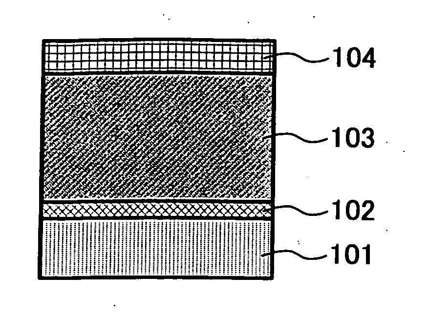
[0234] An undercoat coating liquid, a charge generation coating liquid and charge transport coating liquid, which have the following formulations, were coated in this order on an aluminum cylinder having a diameter of 30 mm and dried to form an undercoat layer of 3.5 μm thick, a CGL of 0.2 μm thick and a CTL of 14 μm thick thereon. The CTL was further coated with a crosslinked surface layer coating liquid having the following formulation by a spray coating method. The coated layer was irradiated with a metal halide lamp at a light quantity of 160 W / cm, a distance of 120 mm and an irradiation intensity of 600 mW / cm2 for 60 sec, and further dried at 130° C. for 30 min to form a crosslinked surface layer having a thickness of 2 μm. Thus prepared electrophotographic photoreceptor was evaluated by the above-mentioned method.

[0235] Undercoat Layer Coating Liquid

Undercoat layer coating liquidAlkyd resin6(BEKKOZOL1307-60-EL from Dainippon Ink & Chemicals, Inc.)Melamine resin4(SUPER BEKKA...

example 2

[0236] An undercoat layer was formed on an aluminum cylinder by the same method as that of Example 1. Next, 1.5 parts of Y-type oxytitanitmphthalocyanine, 1 part of polyester resin (VYLON 200 from Toyobo Co., Ltd.) and 500 parts of a dichloromethane solution having a concentration of 0.5% were pulverized and mixed by a ball mill to prepare a dispersion, and the dispersion was coated on the undercoat layer to form a CGL having a thickness of 0.2 μm thereon. Next, 10 parts of a CTM having the following formula (c) and 10 parts of a polycarbonate resin (PANLITE C-1400 from Teijin Limited) were dissolved in tetrahydrofuran to prepare a CTL coating liquid, and the CTL coating liquid was coated on the CGL to form a CTL having a thickness of 15 μm thereon.

[0237] The procedures of preparation and evaluation of the electrophotographic photoreceptor in Example 1 were repeated except for changing the radical polymerizing monomer having three or more functional groups without a charge transpo...

example 3

[0238] The procedures of preparation and evaluation of the electrophotographic photoreceptor in Example 1 were repeated except for changing the radical polymerizing monomer having three or more functional groups without a charge transport structure included in the crosslinked surface layer coating liquid into the following monomer, the polymerization initiator into the following compound, the thickness of the CTL into 13 μm and the thickness of the crosslinked surface layer into 3 μm.

Radical polymerizing monomer10having three or more functional groupswithout a charge transport structurepentaerythritoltetraacrylate(SR-295 from NIPPON KAYAKU CO., LTD.)having a molecular weight (Mw) of 352,4 functional groups and Mw / 4 of 88Photo polymerization initiator12,4-diethylthioxantone(KAYACURE DETX-S from NIPPON KAYAKU CO., LTD.)


PUM


Abstract

An image forming method including: charging an electrophotographic photoreceptor including: an electroconductive substrate; and a photosensitive layer comprising a crosslinked surface layer on a surface thereof, which is located overlying the electroconductive substrate, irradiating the electrophotographic photoreceptor with imagewise light to form an electrostatic latent image thereon; developing the electrostatic latent image with a toner to form a toner image on the electrophotographic photoreceptor; transferring the toner image onto a transfer material; and fixing the toner image on the transfer material, wherein the photosensitive layer is sensitive to light having a wavelength of from 400 to 450 nm, and the crosslinked surface layer is formed by crosslinking and hardening a radical polymerizing monomer having three or more functional groups without a charge transport structure and a radical polymerizing compound having one functional group with charge transport structure.

Description

BACKGROUND OF THE INVENTION [0001] 1. Field of the Invention [0002] The present invention relates to an image forming method for electrophotographic copiers, printers and facsimiles, and more particularly to an image forming method using a high-resolution electrophotographic photoreceptor capable of recording at not less than 1,200 dpi. [0003] 2. Discussion of the Background [0004] So far, as photosensitive materials for photoreceptors used for electrophotographic image forming methods, various inorganic and organic photosensitive materials have been used. At this point, the “electrophotographic image forming method” mentioned herein means an image forming process of the so-called Carlson process. The electrophotographic image forming method typically includes the following processes: [0005] (1) a photosensitive photoreceptor is charged, for instance, using corona discharging in a dark place; [0006] (2) the photoreceptor is exposed to imagewise light to selectively decay the charge ...

Claims


Application Information

Patent Timeline
Patent Type & Authority Applications(United States)
IPC IPC(8): G03G5/147
CPCG03G5/0546G03G5/0589G03G5/0592G03G5/0596G03G5/073G03G5/0614G03G5/0616G03G5/0637G03G5/071G03G5/0605G03G5/072G03G5/0732G03G5/074G03G5/0745
Inventor OHSHIMA, KOHICHISUZUKI, YASUOSUZUKI, TETSUROSASAKI, MICHITAKA
Owner RICOH KK
Why Eureka
Try Eureka