Stacked via-stud with improved reliability in copper metallurgy
What is Al technical title?
Al technical title is built by PatSnap Al team. It summarizes the technical point description of the patent document.
a copper metallurgy and via-stud technology, applied in the direction of semiconductor/solid-state device details, thin material processing, semiconductor devices, etc., can solve the problems of increasing crack propensity, increasing crack generation, and increasing the proneness of stacked via-studs to cracks, so as to facilitate redundant paths and increase the flexibility of stacked via-studs
Inactive Publication Date: 2006-01-19
GLOBALFOUNDRIES INC
View PDF2 Cites 31 Cited by
Summary
Abstract
Description
Claims
Application Information
AI Technical Summary
This helps you quickly interpret patents by identifying the three key elements:
Problems solved by technology
Method used
Benefits of technology
[0014] It is yet another object of the present invention to provide a semiconductor device having copper interconnections and low strength low-k dielectric with a stacked via-stud that includes at least one cantilever structure, integrated with the stacked via-stud, to allow the mechanical flexibility.
[0037] In this third embodiment, the third conductive structure lies in a perpendicular fashion with respect to the upper and lower conductive structures to facilitate redundant paths connecting the first and second conductive layers via the third conductive layer. Furthermore, the second conductive layer includes a further cantilever structure, the cantilever structures of the second and third conductive structures being interwoven by connecting a cantilever on one conductive structure at a level of interconnection to a bulk portion of a conductive structure on an adjacent level of interconnection, thereby increasing flexibility of stacked via-studs between interconnection levels.
Problems solved by technology
The continuing trend of dimensional shrinkage (smaller D) and increased wiring levels (larger H) in multilevel interconnections lead to much higher H to D ratios, thereby making the stacked via-studs of present and future interconnection wiring schemes increasingly more prone to cracks.
The crack propensity also increases with the range of temperature cycles and the number of cycles, showing that cracks are generated by metal fatigue, a phenomenon not seen before in integrated circuit wiring.
The negligibly small compressive stress in low-k materials, along with the large thermal expansion mismatch between copper and low-k dielectric, e.g., SiLK, are root causes for the observed fatigue failure.
All of Saran's schemes involve short length metal studs bounded on top and bottom by a dense dielectric material; such schemes are not beneficial when the studs are long, for example, in the case of stacked via-studs as discussed above.
Method used
Image
Click on the blue label to locate the original text in one second.
Reading with bidirectional positioning of images and text.
Examples
Embodiment Construction
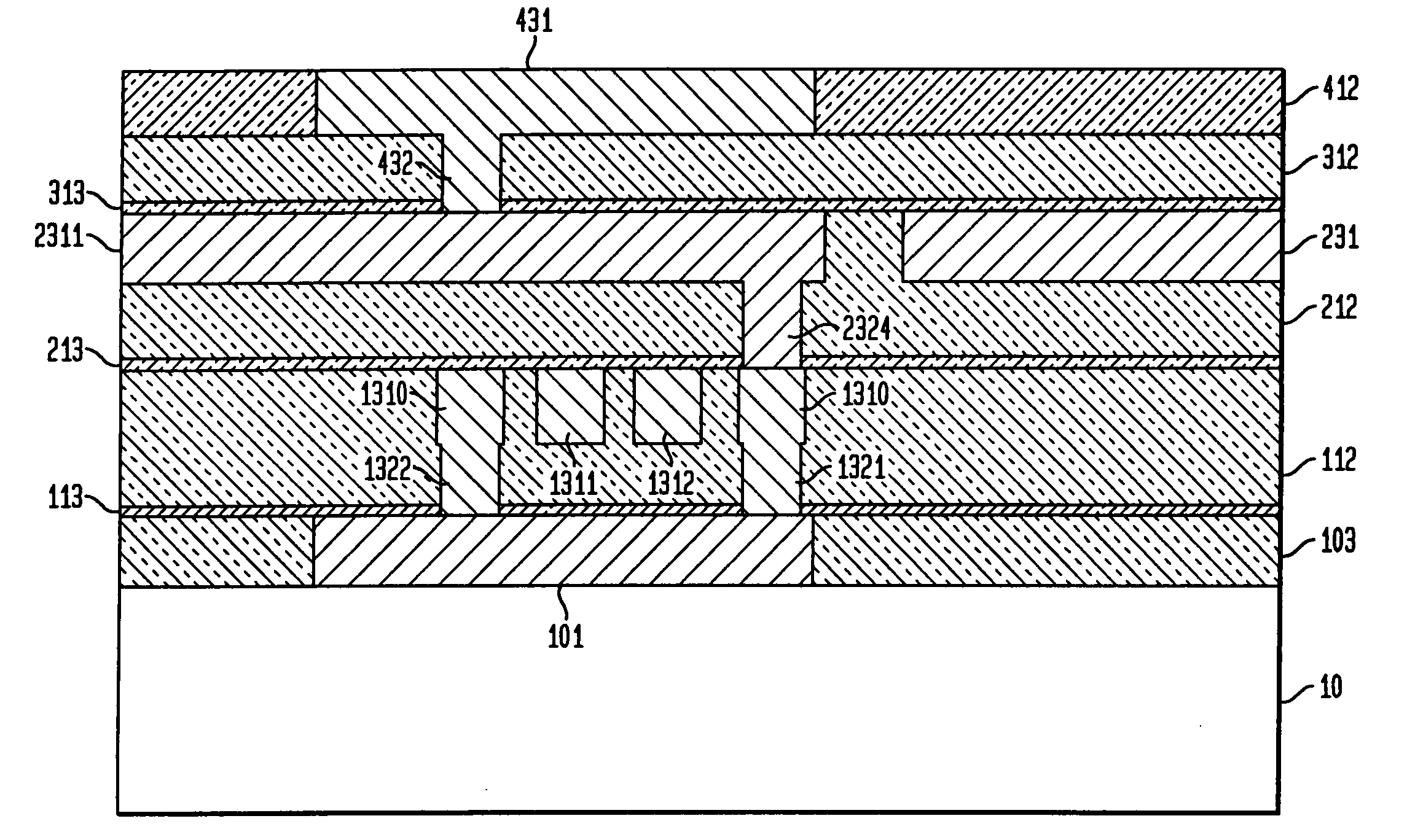
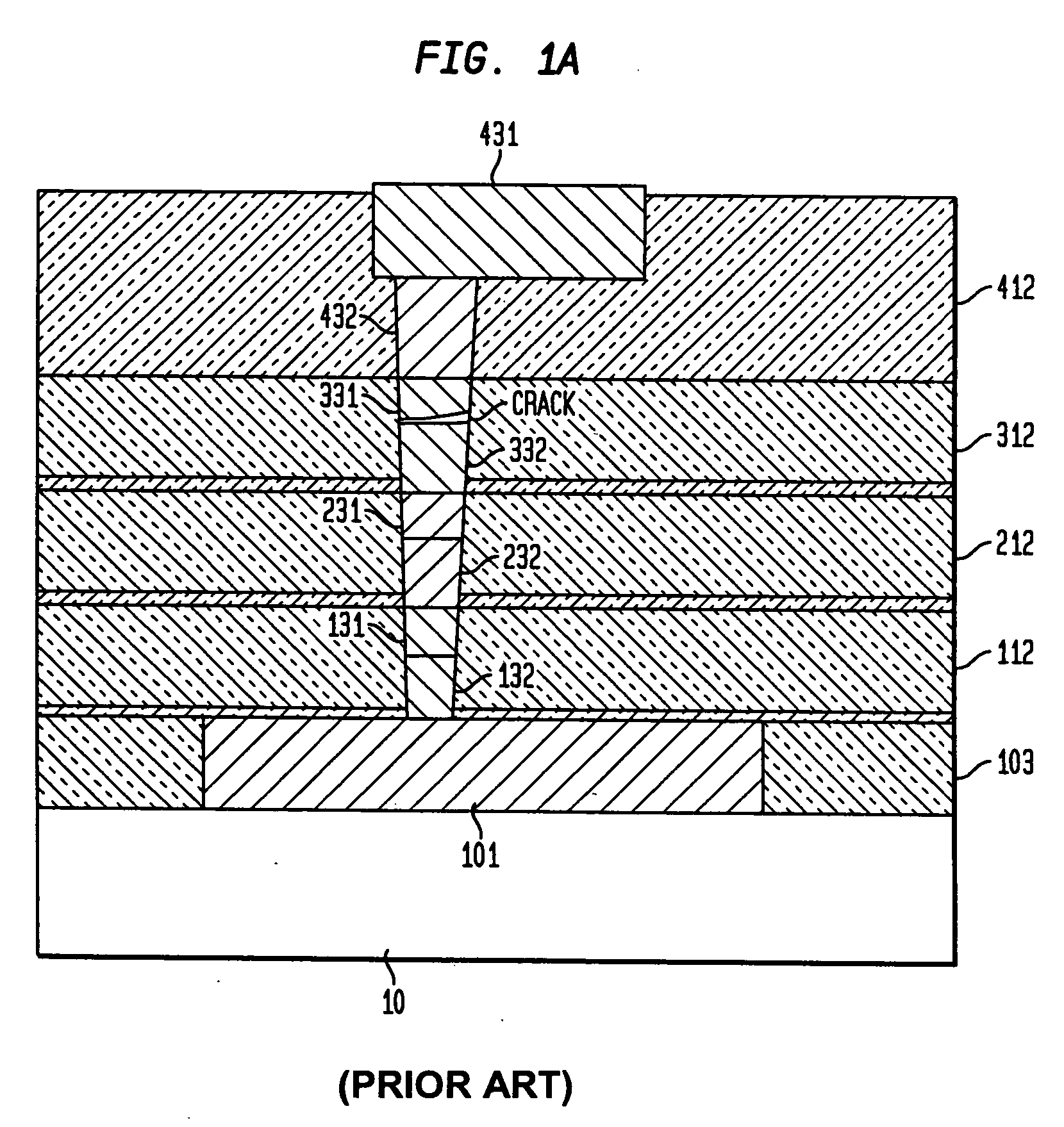
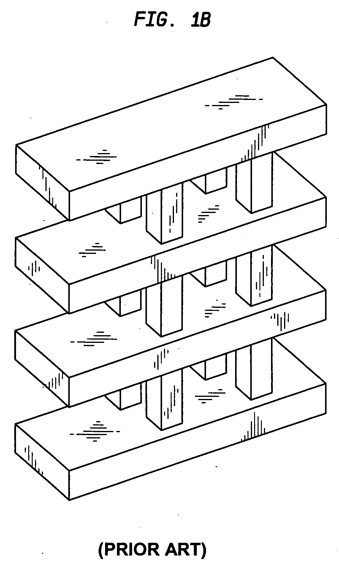
[0048] The present invention is generally related to methods for forming metal filled via-studs and conductor lines on a substrate where the via-studs and conductor lines are formed using a dual damascene method, and preferably copper metallurgy and low-k dielectric material. The present invention has particular relevance to stacked via-stud schemes which particularly use low strength low-k dielectric materials and incorporate a cantilever structure within the stacked via-stud which may serve as an effective thermal fatigue crack stop.
[0049] Particularly referring to FIG. 2, there is shown a semiconductor substrate 10 above which a sequence of dielectric layers 111, 112, 113 is deposited, subsequently patterned and metallized to form a first level of interconnection. It should be understood that a plurality of semiconductor devices may be formed in the substrate and, although not shown, are provided with a local interconnect line 101, typically tungsten with underlayers of titanium...
PUM
Property
Measurement
Unit
thickness
aaaaa
aaaaa
thickness
aaaaa
aaaaa
thickness
aaaaa
aaaaa
Abstract
A multilevel semiconductor integrated circuit (IC) structure including a first interconnect level including a layer of dielectric material over a semiconductor substrate, the layer of dielectric material comprising a dense material for passivating semiconductor devices and local interconnects underneath; multiple interconnect layers of dielectric material formed above the layer of dense dielectric material, each layer of dielectric material including at least a layer of low-k dielectric material; and, a set of stacked via-studs in the low-k dielectric material layers, each of said set of stacked via studs interconnecting one or more patterned conductive structures, a conductive structure including a cantilever formed in the low-k dielectric material. The dielectric layer of each of the multiple interconnection levels includes a soft low-k dielectric material, wherein the cantilever and set of stacked via-studs are integrated within the soft low-k dielectric material to increase resistance to thermal fatigue crack formation. In one embodiment, each of the set of stacked via-studs in the low-k dielectric material layers is provided with a cantilever, such that the cantilevers are interwoven by connecting a cantilever on one level to a bulk portion of the conductor line on adjacent levels of interconnection, thereby increasing flexibility of stacked via-studs between interconnection levels.
Description
BACKGROUND OF THE INVENTION [0001] 1. Field of the Invention [0002] The present invention relates generally to a new semiconductor process and integrated circuit structure, and more particularly, to a new process and structure which provides stacked via-studs, in multilevel interconnection wiring of semiconductor devices with high conductivity copper metallurgy and low-k dielectric, with improved mechanical stability under large thermal excursions. [0003] 2. Description of the Prior Art [0004] In order to meet the ever increasing demand for increased device density and performance, a semiconductor technology consisting of a low-k dielectric material and an interconnection wiring of copper metallurgy, defined by a dual damascene method, is the present day choice. Because, dry air has the theoretically lowest dielectric constant of one (1), most low-k materials such as aerogels, hydrogen silsesquioxane (HSQ), fluorinated organic polymers (e.g., SiLK, a trade mark of Dow chemical Co., ...
Claims
Application Information
Patent Timeline
Application Date:The date an application was filed.
Publication Date:The date a patent or application was officially published.
First Publication Date:The earliest publication date of a patent with the same application number.
Issue Date:Publication date of the patent grant document.
PCT Entry Date:The Entry date of PCT National Phase.
Estimated Expiry Date:The statutory expiry date of a patent right according to the Patent Law, and it is the longest term of protection that the patent right can achieve without the termination of the patent right due to other reasons(Term extension factor has been taken into account ).
Invalid Date:Actual expiry date is based on effective date or publication date of legal transaction data of invalid patent.
Patent Type & Authority Applications(United States)