Process for fabricating non-volatile memory by tilt-angle ion implantation

Inactive Publication Date: 2006-01-26
CHUNG YUAN CHRISTIAN UNIVERSITY
View PDF2 Cites 3 Cited by
  • Summary
  • Abstract
  • Description
  • Claims
  • Application Information

AI Technical Summary

Benefits of technology

[0010] One object of the invention is to provide a process for fabricating non-volatile memory by tilt-angle ion implan

Problems solved by technology

However, the floating gate device 1 can store only one bit so that its production cost is correspondingly increased and hence exhibit substantially no economical benefit.
Unfortunately, the charge trapping device 2 shows a big problem on retention time, because oxides 21 in the underlying layer might capture positive charge therein during programming that may lower the energy barrier of the underlying oxide layer 21 and as a resu

Method used


Image

  • Process for fabricating non-volatile memory by tilt-angle ion implantation
  • Process for fabricating non-volatile memory by tilt-angle ion implantation
  • Process for fabricating non-volatile memory by tilt-angle ion implantation

Examples


Embodiment Construction

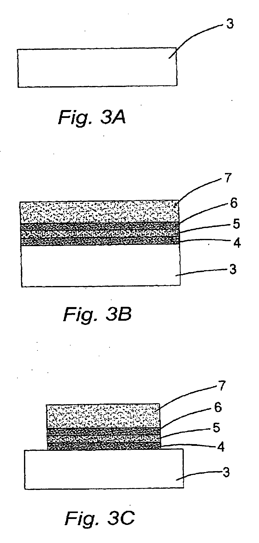
[0018] Referring to FIGS. 3A-3F, a process for fabricating non-volatile memory by tilt-angle ion implantation according to the invention comprises the steps of:

[0019] step 1: providing a wafer substrate 3 (FIG. 3A);

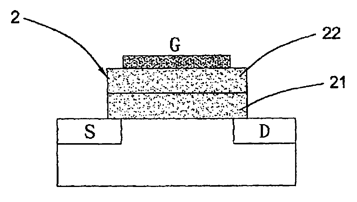
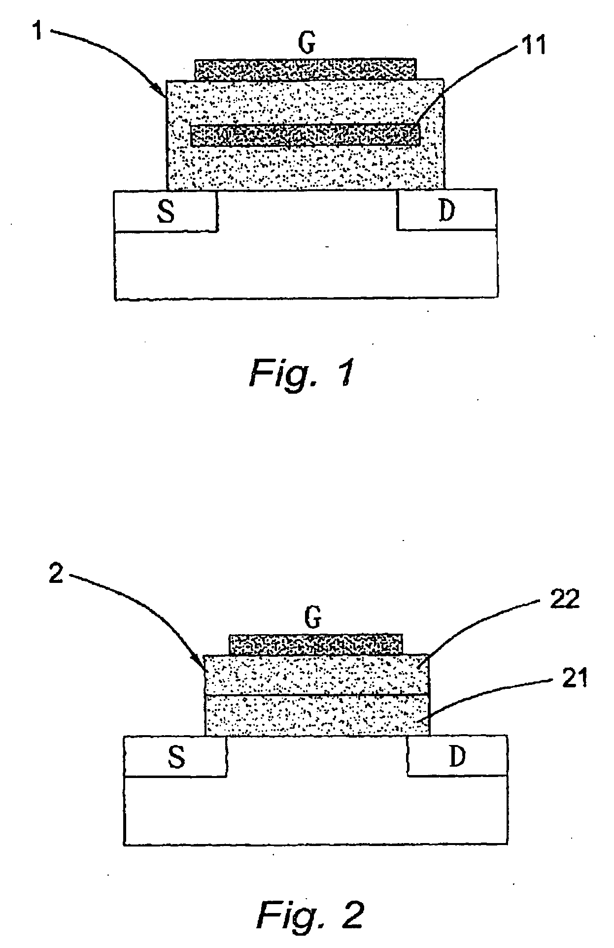
[0020] step 2: depositing over the wafer substrate 3 successively a first oxide layer 4, nitride layer 5, an upper second oxide layer 6, and a gate 7, in a manner that a gate dielectric layer (oxide-nitride-oxide (ONO)) is formed over the wafer substrate 3 (FIG. 3B), wherein said nitride layer 5 can store two bits at the same time; said first and second oxide layers 4, 6 may be silicon oxide; said gate layer 7 is a polysilicon layer; and said nitride layer 5 is silicon nitride;

[0021] step 3: forming gate pattern by photoresist developing, and removing both ends of the gate dielectric layer by directional etching to expose said first oxide layer or said substrate (FIG. 3C);

[0022] step 4: removing the photoresist and implanting sideling within said nitride layer 5 heter...


PUM


Abstract

A process for fabricating non-volatile memory by tilt-angle ion implantation comprises essentially the steps of implanting sideling within a nitride dielectric layer heterogeneous elements such as, for example, Ge, Si, N2, O2, and the like, for forming traps capable of capturing more electrons within the nitride dielectric layer such that electrons can be prevented from binding together as the operation time increased; etching off both ends of the original upper and underlying oxide layers to reduce the structural destruction caused by the implantation of heterogeneous elements; and finally, depositing an oxide gate interstitial wall to eradicate electron loss and hence promote the reliability of the device.

Description

BACKGROUND OF THE INVENTION [0001] 1. Field of the Invention [0002] The invention relates to a process for fabricating non-volatile memory by tilt-angle ion implantation, and in particular, to a process for fabricating non-volatile memory by tilt-angle ion implantation characterized in that, in addition to increase the retention time of the memory, it can avoid merge of electrons due to prolonged operation. [0003] 2. Description of the Prior Art [0004] Recently, the role of the flash memory device in the development and fabrication of the semiconductor device has becomes more and more important. As portable electronic products increasingly prevail, the modification and portability of data has a pivotal function in these products, and accordingly, a flash memory has its competitive advantage over other devices. [0005] Referring to FIGS. 1 and 2, a schematic structure of a conventional non-volatile memory is shown to be composed of two different structures: a floating gate device 1 (F...

Claims


Application Information

Patent Timeline
IPC IPC(8): H01L21/8238
CPCH01L21/28282H01L29/7923H01L29/4234H01L29/40117
Inventor JENG, ERIK S.CHOU, WU-CHINGWU, LI-KANGLI, CHIEN-CHEN
Owner CHUNG YUAN CHRISTIAN UNIVERSITY
Why Eureka
Try Eureka