

Thermoelectric conversion material, thermoelectric conversion device and manufacturing method thereof
a technology of thermoelectric conversion device and thermoelectric conversion material, which is applied in the manufacture/treatment of thermoelectric devices, crystal growth process, transportation and packaging, etc., can solve the problems of difficult to produce pores separated by alumina walls, difficult to form pores of a cross-sectional size (or diameter) less than 7 nm, etc., and achieves a higher thermoelectric figure of merit
- Summary
- Abstract
- Description
- Claims
- Application Information
AI Technical Summary
Benefits of technology
Problems solved by technology
Method used
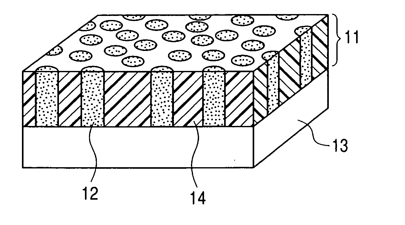
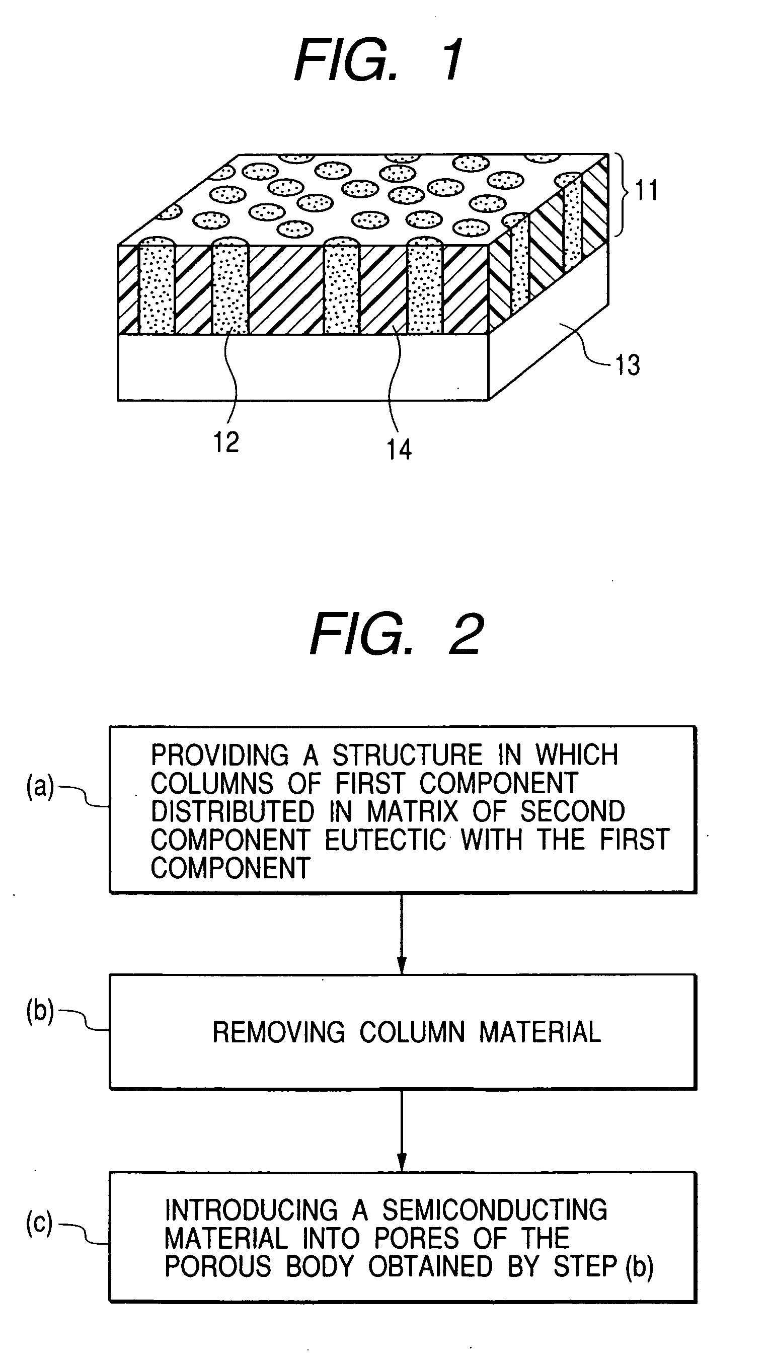
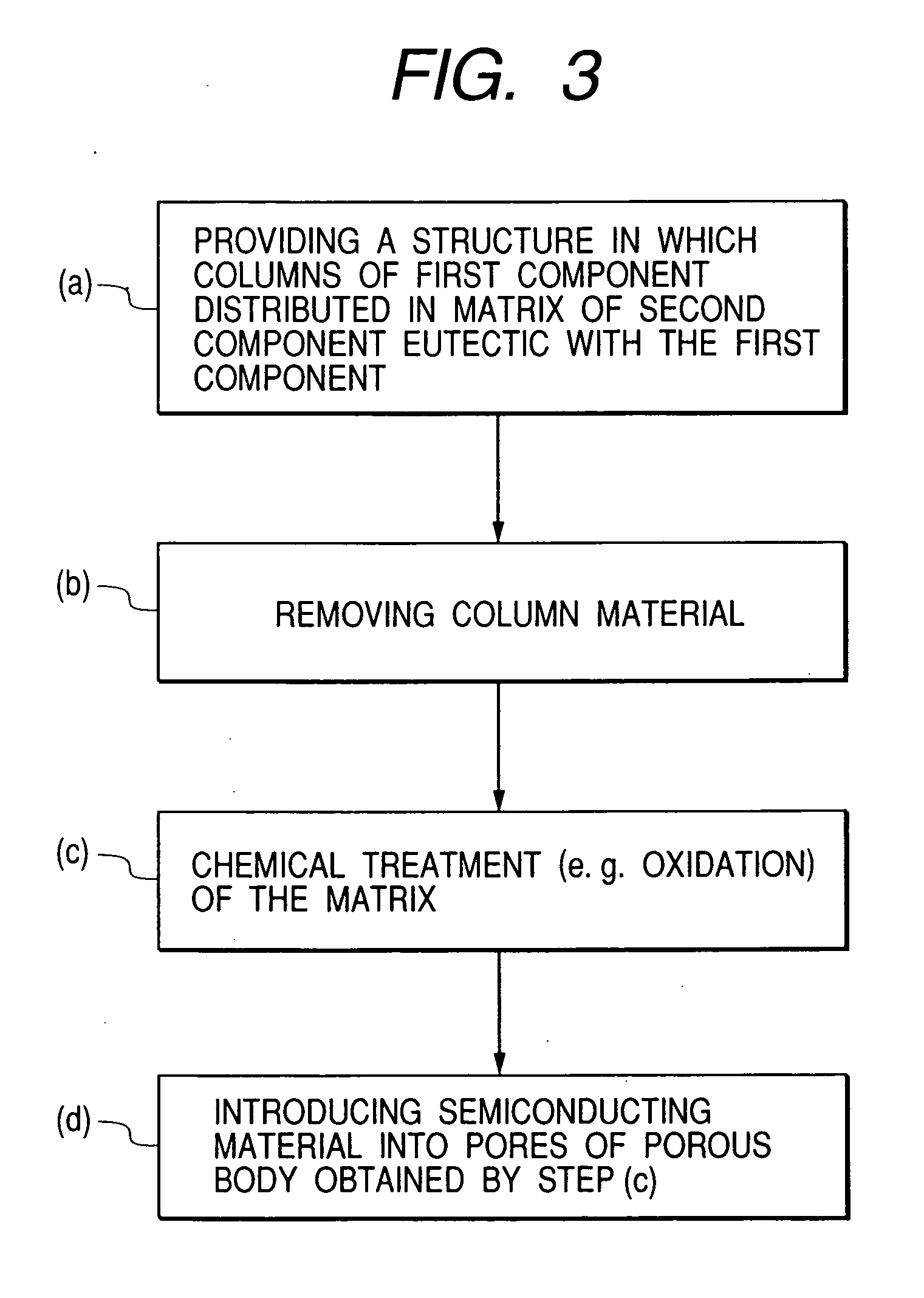
Image

Examples
example 1
[0088] In this example, a thermoelectric conversion material was produced in which the porous body having the columnar pores was amorphous silicon, and the semiconductor filled into the pores was BiTe.
[0089] First, an aluminum-silicon mixture film of about 200 nm thick containing 37 atomic % of silicon to the total of aluminum and silicon was formed by magnetron sputtering on a silicon substrate on which 20 nm of tungsten was deposited as an electrode for electrodeposition of BiTe (thermoelectric material). As a target, a six 15-mm square silicon chips are placed on a circular aluminum target of 4 inches in diameter (101.6 mm). Sputtering conditions employed were such that supply was used with an Ar flow of 50 sccm, a discharging pressure of 0.7 Pa and input power of 1 kW. The substrate temperature was room temperature (25° C.).
[0090] The aluminum-silicon mixture film thus obtained was observed by FE-SEM (Field Emission-Scanning Electron Microscope). When the surface was viewed fr...
example 2
[0095] In this example, a thermoelectric conversion material was produced in which the main component of the porous body having the columnar pores was silicon oxide, and the semiconductor filled into the pores was BiTe.
[0096] First, an aluminum-silicon mixture film of about 200 nm thick containing 37 atomic % of silicon to the total of aluminum and silicon was formed by magnetron sputtering on a silicon substrate on which 20 nm of tungsten was deposited as an electrode for electrodeposition of BiTe (thermoelectric material). As a target, a six 15-mm square silicon chips are placed on a circular aluminum target of 4 inches in diameter (101.6 mm). Sputtering conditions employed were such that supply was used with an Ar flow of 50 sccm, a discharging pressure of 0.7 Pa and input power of 1 kW. The substrate temperature was room temperature (25° C.).
[0097] The aluminum-silicon mixture film thus obtained was observed with an FE-SEM (Field Emission-Scanning Electron Microscope) to find ...
example 3
[0102] In this example, a thermoelectric conversion material was produced in which the material of the porous body having the columnar pores was germanium, and the semiconductor filled into the pores was BiSb.
[0103] First, an aluminum-germanium mixture film of about 200 nm that contained 37 atomic % of germanium relative to the sum amount of aluminum and germanium was formed by magnetron sputtering, on a silicon substrate on which tungsten of 20 nm thick had been deposited thereon as the electrode for electrodeposition of BiSb (thermoelectric material). A target was used in which four 15-mm square germanium chips are placed on a circular aluminum target having a diameter of 4 inches (101.6 mm). Sputtering conditions were employed where RF power supply was used with an Ar flow: 12 sccm, a discharging pressure: 0.05 Pa and input power: 60 W. The substrate temperature was room temperature (25° C.).
[0104] The aluminum-germanium mixture film thus obtained was observed with an FE-SEM, a...
PUM
 Abstract
Description
Claims
Application Information