Stretchable semiconductor elements and stretchable electrical circuits

a technology of stretchable electrical circuits and semiconductor elements, applied in the direction of sustainable manufacturing/processing, semiconductor/solid-state device details, final product manufacturing, etc., can solve the problems of inability to achieve incompatibility with most plastic materials, and well-developed methods of making conventional silicon-based electronic devices. , to achieve the effect of preventing the complete release of relief structur

Active Publication Date: 2006-02-23
THE BOARD OF TRUSTEES OF THE UNIV OF ILLINOIS
View PDF10 Cites 532 Cited by
  • Summary
  • Abstract
  • Description
  • Claims
  • Application Information

AI Technical Summary

Benefits of technology

[0065] In another embodiment, the present invention provides a method for fabricating a printable semiconductor element connected to a mother wafer via one or more alignment maintaining elements comprising the steps of: (1) providing the mother wafer having an external surface, the wafer comprising an inorganic semiconductor material; (2) masking a selected region of the external surface by applying a mask; (3) etching the external surface of the wafer, thereby generating a relief structure and at least one exposed surface of the wafer, wherein the relief structure has a masked side and one or more unmasked sides; (4) etching the exposed surfaces of the wafer; and (5) stopping etching of the exposed structure so that complete release of the relief structure is prevented, thereby fabricating the printable semiconductor element connected to a mother wafer via one or more alignment maintaining elements. In one embodiment of this method the printable semiconductor element has a peanut shape with a first end and a second end, wherein the alignment maintaining elements connect the first and second ends of the printable semiconductor element to the mother wafer. In another embodiment of this method the printable semiconductor element has a ribbon shape with a first end and a second end, wherein the alignment maintaining elements connect the first and second ends of the printable semiconductor element to the mother wafer.

Problems solved by technology

Second, the inherent flexibility of these substrate materials allows them to be integrated into many shapes providing for a large number of useful device configurations not possible with brittle conventional silicon based electronic devices.
For example, bendable flexible electronic devices are expected to enable fabrication of new devices, such as electronic paper, wearable computers and large-area high resolution displays, that are not easily achieved with established silicon based technologies.
The design and fabrication of flexible electronic devices exhibiting good electronic performance, however, present a number of significant challenges.
First, the well developed methods of making conventional silicon based electronic devices are incompatible with most plastic materials.
In addition, most inorganic semiconductors are not intrinsically soluble in convenient solvents that would allow for solution based processing and delivery.
Second, although many amorphous silicon, organic or hybrid organic-inorganic semiconductors are compatible with incorporation into plastic substrates and can be processed at relatively low temperatures, these materials do not have electronic properties capable of providing integrated electronic devices capable of good electronic performance.
As a result of these limitations, flexible electronic devices are presently limited to specific applications not requiring high performance, such as use in switching elements for active matrix flat panel displays with non-emissive pixels and in light emitting diodes.
While this class of flexible electronic devices provides enhanced device electronic performance characteristics, use of pulsed laser annealing limits the ease and flexibility of fabrication of such devices, thereby significantly increasing costs.
This device field effect mobility is several orders of magnitude lower than the device field effect mobilities of conventional single crystalline inorganic thin film transistors, and is likely due to practical challenges in aligning, densely packing and electrically contacting discrete nanowires or nanoribbons using the methods and device configurations disclosed in Duan et al.
Particularly, the use of organic end groups to stabilize nanocrystal solutions and prevent agglomeration may impede establishing good electrical contact between adjacent nanoparticles that is necessary for providing high device field effect mobilities.
However, such motion is expected to generate mechanical strain on the individual rigid transistor device components.
This mechanical strain may induce damage to individual components, for example by cracking, and also may degrade or disrupt electrical contact between device components.

Method used


Image

  • Stretchable semiconductor elements and stretchable electrical circuits
  • Stretchable semiconductor elements and stretchable electrical circuits
  • Stretchable semiconductor elements and stretchable electrical circuits

Examples


example 1

Thin Film Transistor Having a Printable Semiconductor Element

[0167] The ability of printable semiconductor elements of the present invention to provide semiconductor channels in thin film transistors was verified by experimental studies. Specifically, it is a goal of the present invention to provide thin film transistors capable of fabrication on a flexible plastic substrates by printing methods. Further, it is a goal of the present invention to provide high performance thin film transistors on plastic substrates having field effect mobilities, on-off ratios and threshold voltages similar to or exceeding thin film transistors fabricated by convention high temperature processing methods.

[0168]FIG. 7 presents an optical micrograph image of a thin film transistor having a printable semiconductor element. The illustrated transistor 531 comprises source electrode 532, drain electrode 533, printable semiconductor element 534, dielectric (not shown in the micrograph in FIG. 7) and gate e...

example 2

Stretchable Printable Semiconductor Elements

[0179] The present invention provides stretchable printable semiconductor elements capable of providing good performance when stretched, flexed or deformed. Further, stretchable printable semiconductor elements of the present invention may be adapted to a wide range of device configurations to provide fully flexible electronic and optoelectronic devices.

[0180]FIG. 12 provides an atomic force micrograph showing a stretchable printable semiconductor element of the present invention. The stretchable printable semiconductor element 700 comprises a flexible substrate 705 having a supporting surface 710 and a bent semiconductor structure 715 having a curved internal surface 720. In this embodiment, at least a portion of the curved internal surface 720 of bent semiconductor structure 715 is bonded to the supporting surface 710 of the flexible substrate 705. The curved internal surface 720 may be bonded supporting surface 710 at selected points ...

example 3

Methods of Making Printable Semiconductor Elements

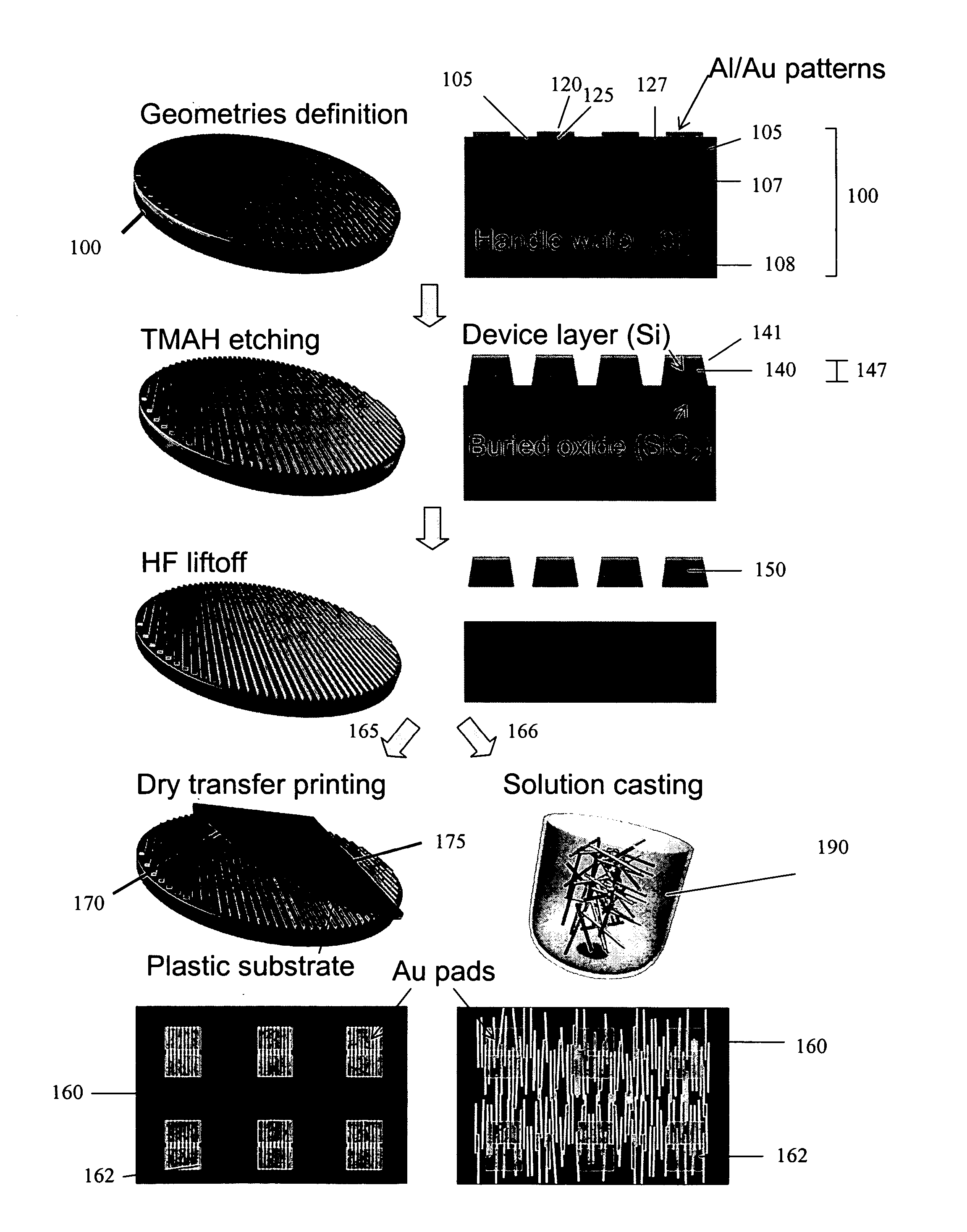
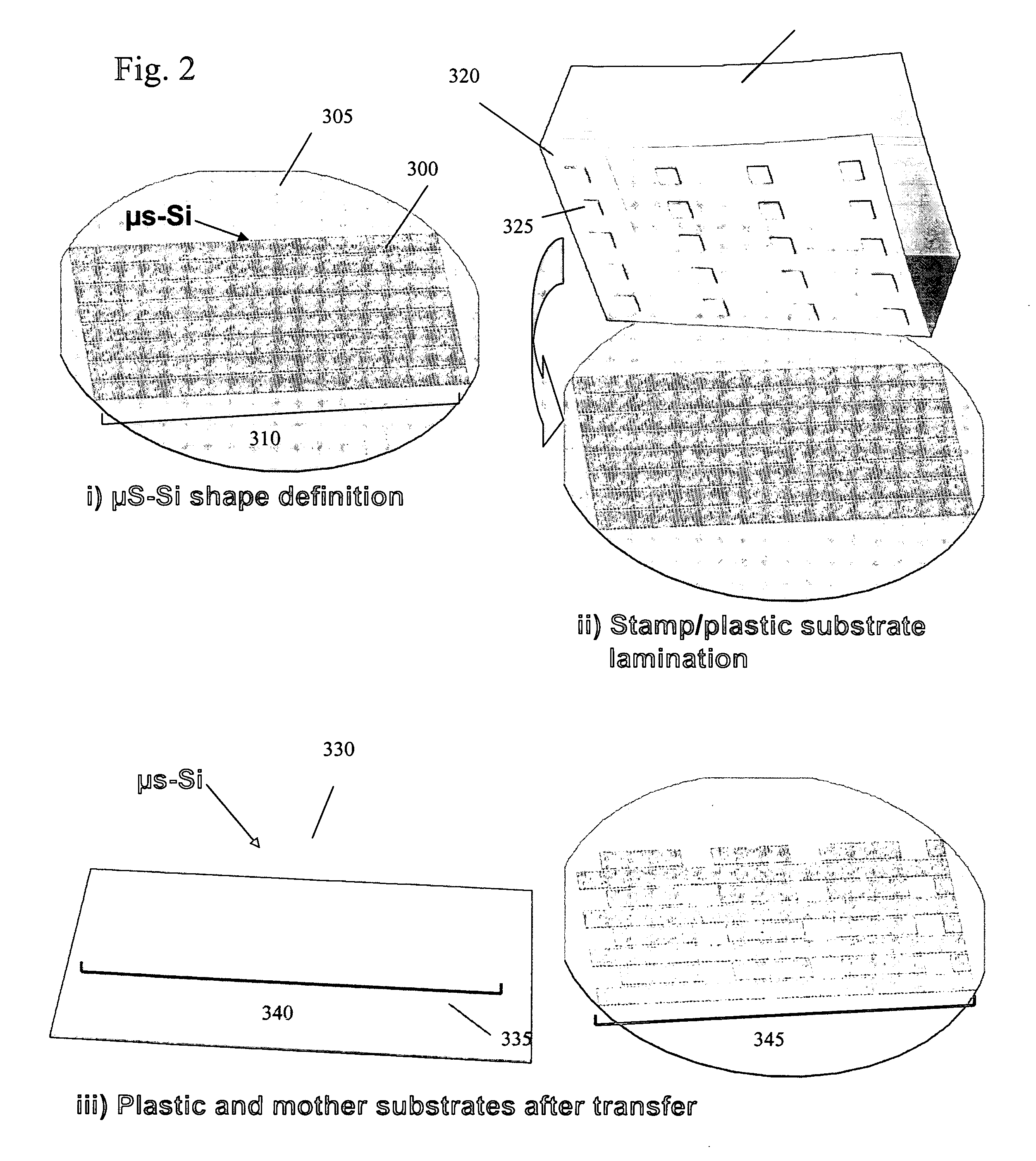
[0186] The present invention provides methods of making printable semiconductor elements from a wide range of starting materials, including single crystalline wafers, silicon on substrate wafers, germanium wafers, thin films of polycrystalline silicon and ultra thin silicon wafers. Particularly, the present invention provides low cost methods of making large numbers of printable semiconductors in selected orientations and relative positions.

[0187]FIG. 18A shows an exemplary method for making printable semiconductor elements from a Si—Ge epi substrate. In this method, selective regions of a Si epi layer are masked by depositing a mask material, such as a thin films comprising a metal, SiO2 or SiN. This masking step defines shape and some of the physical dimensions (e.g. length and width for a ribbon) of the printable semiconductor elements to be fabricated. The exposed Si surface of the Si—Ge epi substrate is anisotropically etched ...


PUM

PropertyMeasurementUnit
thicknessaaaaaaaaaa
thicknessaaaaaaaaaa
thicknessaaaaaaaaaa

Abstract

The invention provides methods and devices for fabricating printable semiconductor elements and assembling printable semiconductor elements onto substrate surfaces. Methods, devices and device components of the present invention are capable of generating a wide range of flexible electronic and optoelectronic devices and arrays of devices on substrates comprising polymeric materials. The present invention also provides stretchable semiconductor structures and stretchable electronic devices capable of good performance in stretched configurations.

Description

CROSS REFERENCE TO RELATED APPLICATION [0001] This application claims priority under 35 U.S.C. 119(e) to U.S. Provisional Patent Application Nos. 60 / 577,077, 60 / 601,061, 60 / 650,305, 60 / 663,391 and 60 / 677,617 filed on Jun. 4, 2004, Aug. 11, 2004, Feb. 4, 2005, Mar. 18, 2005, and May 4, 2005, respectively, which are hereby incorporated by reference in their entireties to the extent not inconsistent with the disclosure herein.STATEMENT REGARDING FEDERALLY SPONSORED RESEARCH OR DEVELOPMENT [0002] This invention was made, at least in part, with United States governmental support awarded by Department of Energy under Grant No. DEFG02-91ER45439 and the Defense Advanced Projects Agency under Contract F8650-04-C-710. The United States Government has certain rights in this invention.BACKGROUND OF INVENTION [0003] Since the first demonstration of a printed, all polymer transistor in 1994, a great deal of interest has been directed at a potential new class of electronic systems comprising flexi...

Claims


Application Information

Patent Timeline
Patent Type & Authority Applications(United States)
IPC IPC(8): H01L31/0312B81C1/00H01L29/06H01L29/786H01L31/18
CPCB81C2201/0185B82Y10/00H01L29/0665H01L29/0673H01L29/0676H01L29/068H01L29/78603H01L29/78681H01L29/78696H01L31/0392H01L31/18H01L31/1804Y10S977/724Y10S977/707H01L2924/12041Y02E10/547H01L21/02521H01L21/308H01L29/12H01L2224/83005H01L2224/03614H01L2224/80862H01L24/03H01L24/05H01L24/08H01L24/29H01L24/32H01L21/6835H01L24/80H01L24/83H01L24/94H01L24/97H01L2221/68368H01L2221/68381H01L2224/0332H01L2224/0345H01L2224/0362H01L2224/05073H01L2224/05082H01L2224/05124H01L2224/05144H01L2224/05155H01L2224/05166H01L2224/05552H01L2224/05553H01L2224/05554H01L2224/05555H01L2224/05644H01L2224/05666H01L2224/08225H01L2224/2919H01L2224/32225H01L2224/80006H01L2224/80121H01L2224/80895H01L2224/83121H01L2224/83192H01L2224/83193H01L2224/8385H01L2224/83862H01L2224/9202H01L2224/94H01L2224/97H01L2924/10253H01L2924/10329H01L2924/15159H01L2924/15162H01L2924/1579H01L29/04H01L29/06H01L27/1285H01L27/1292H01L2924/13091H01L2924/1306H01L2924/1461H01L21/02603H01L21/02628H01L2924/1305H01L2924/00014H01L2224/80H01L2224/83H01L2924/00012H01L2224/03H01L2924/0665H01L2924/01032H01L2924/00H01L27/1214H01L31/03926H01L31/1864H01L31/1896H01L2224/95H01L2924/12042H01L2924/12036H01L2924/12032H01L2924/12044H01L2924/12043H01L2924/15788H01L2924/13063H01L2924/14H01L2924/13055Y02P70/50H01L27/00H01L21/322H01L23/02H01L29/76H01L33/0093H01L25/0753H01L33/007H01L33/32
Inventor ROGERS, JOHN A.KHANG, DAHL-YOUNG
Owner THE BOARD OF TRUSTEES OF THE UNIV OF ILLINOIS
Why Eureka
Try Eureka