Method for depositing porous films

a technology of porous films and processing methods, applied in the direction of basic electric elements, electrical apparatus, semiconductor devices, etc., can solve the problems of less than desired final dielectric constant, not ready for manufacturing considerations, and the amorphous carbon technology is still very immature, so as to facilitate and optimally control the codeposition and selective silicon removal steps

Inactive Publication Date: 2006-02-23
MAK CECILIA Y +1
View PDF12 Cites 47 Cited by
  • Summary
  • Abstract
  • Description
  • Claims
  • Application Information

AI Technical Summary

Benefits of technology

[0017] There are three salient features in this invention: 1) the codeposition of the silica (or the host matrix material in general) with silicon, 2) the exposure of the codeposit film to a selective silicon removal reagent during the silicon removal step, and 3) a methodology to facilitate and optimally control the codeposition and selective silicon removal steps.

Problems solved by technology

However, amorphous carbon technology is still very immature and for now is not ready for manufacturing considerations.
However, the oxycarbide films are prone to carbon depletion in subsequent processing, resulting in a less than desired final dielectric constant.
Furthermore, the incorporation of carbon in silica introduces many process complications, particularly in etching, chemical mechanical polishing, and cleaning.
Consequently, implementation has been formidable and costly.
Compared to silicon dioxide, these films are generally mechanically softer and less thermally stable.
They also tend to take up moisture so additional cap layers are often required to protect them.
Because of the different properties, there are many restrictions in conventional processing and modifications are frequently needed to accommodate these films in process integration.
Sol-gel techniques, however, require meticulous gellation and drying.
Their different modes of processing, process control, and integration schedules are incompatible with semiconductor device manufacturing.
However, like other porogen techniques, this CVD technique is based on volatilizing organic species, and there are concerns for residual outgassing if the organic species that are supposed to be removed are not removed entirely.
Moreover, process integration complications associated with processing carbon-containing oxide films still remain, as discussed earlier.

Method used


Image

  • Method for depositing porous films
  • Method for depositing porous films
  • Method for depositing porous films

Examples


Embodiment Construction

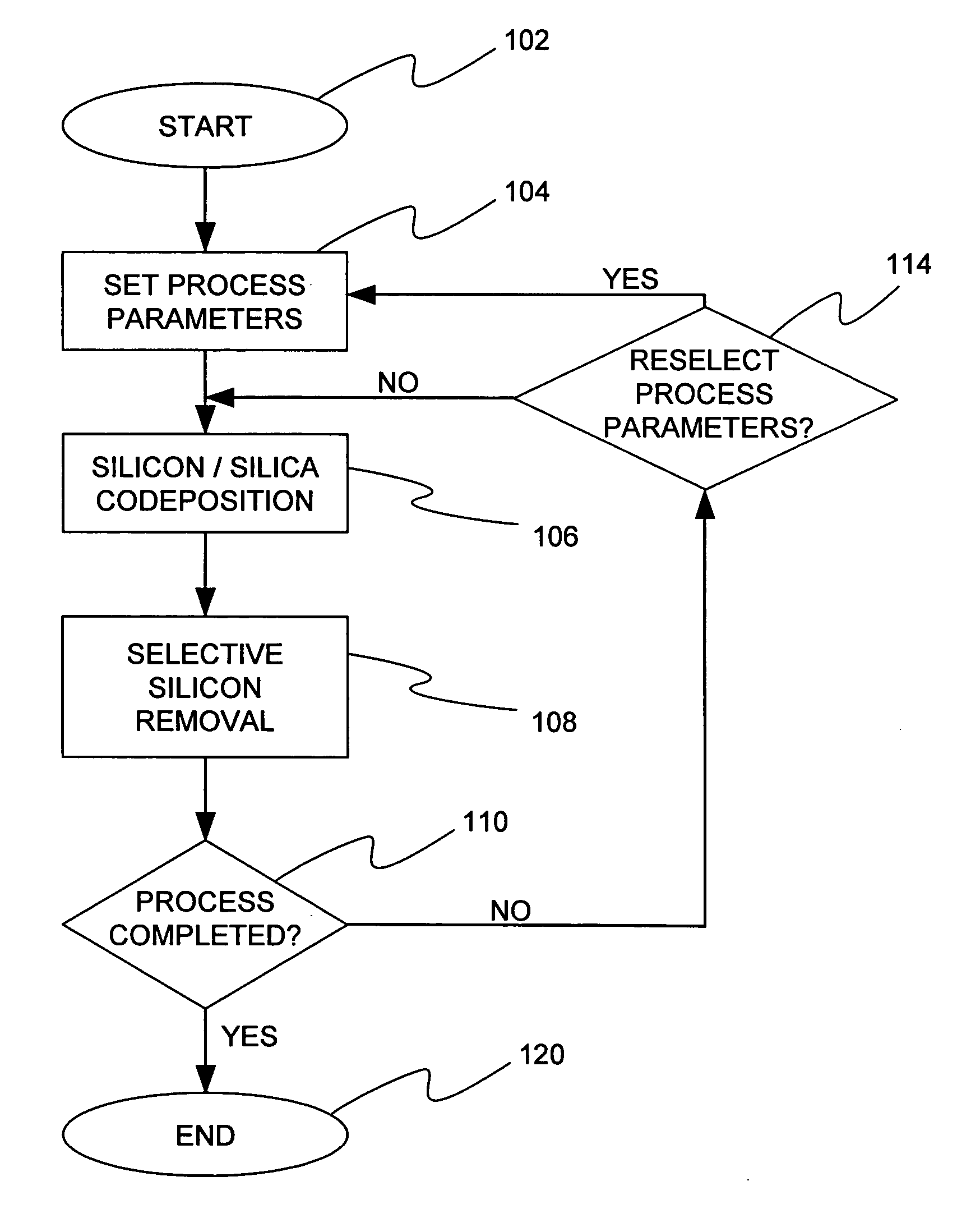
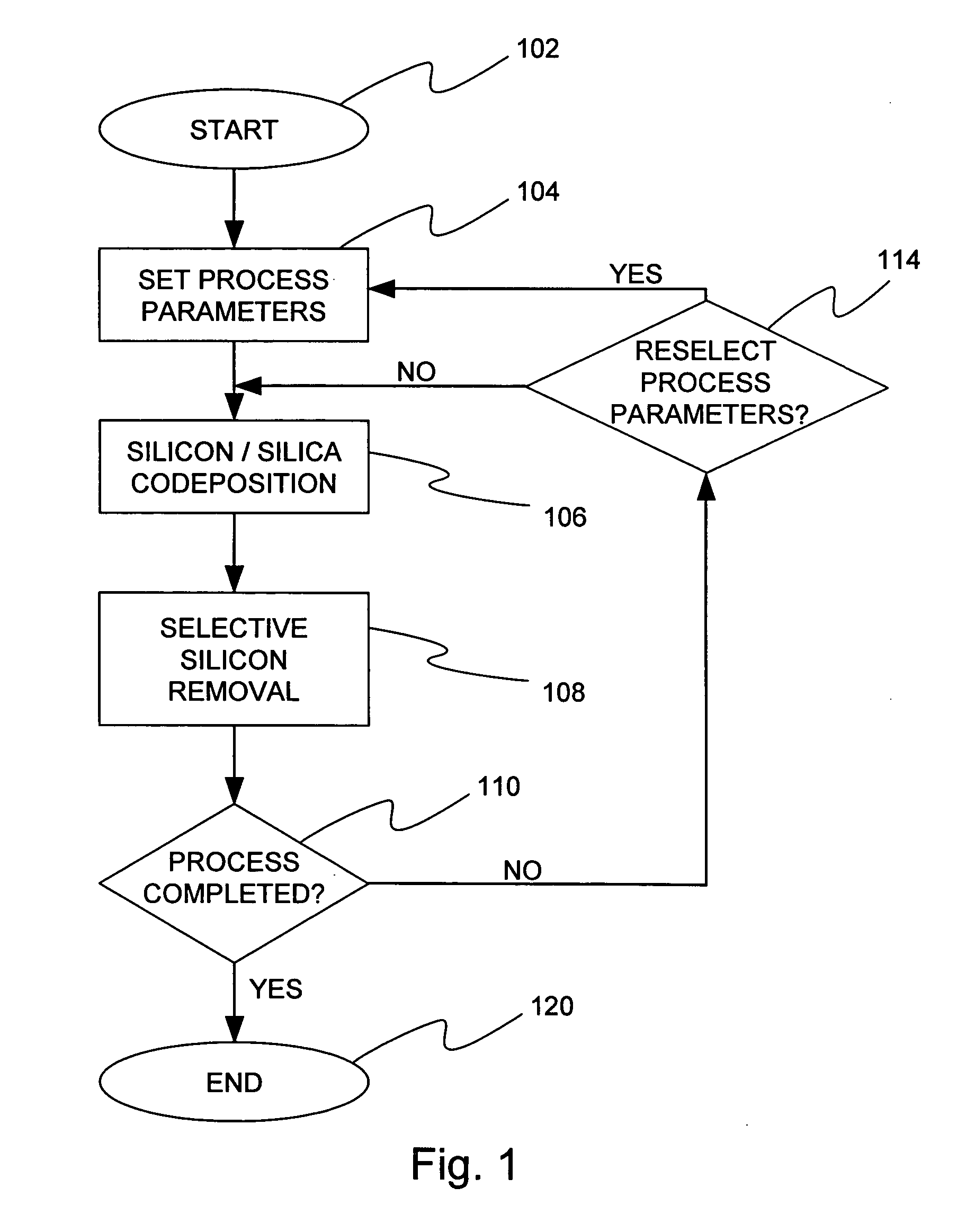
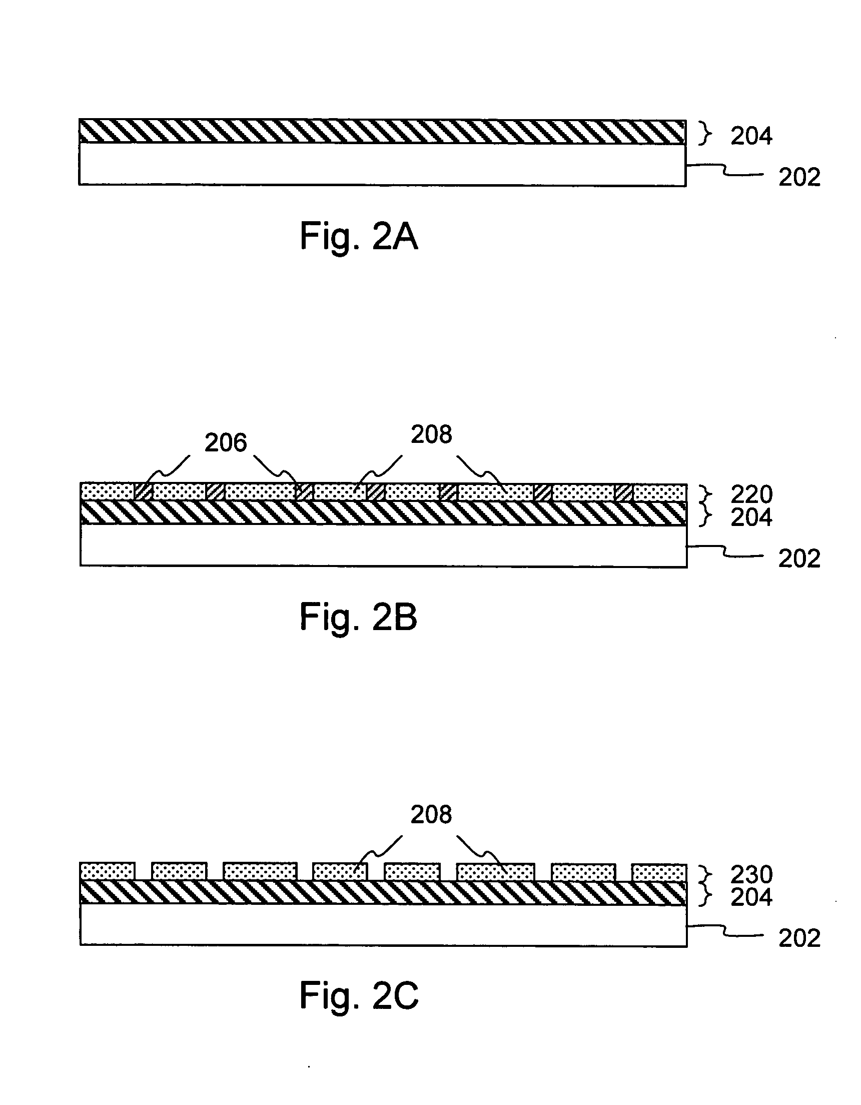
[0031] The present invention provides a process method for forming porous silica or doped silica films on a substrate for semiconductor integrated circuits fabrication. The method is also generally applicable for forming porous films of other host matrix materials using the features described in the disclosure. For simplicity in discussion, we shall focus the description primarily on porous silica films.

[0032] According to the invention, the method entails a cyclic process scheme to form the film. In each cycle, a thin layer of silica and silicon or doped silica and silicon are first codeposited. (The codeposited film may be commonly viewed as a silicon-rich oxide or silicon-rich doped oxide). Then, the silicon is selectively removed from the codeposit to create a porous silica structure. The processing steps are repeated alternately to build up the thickness of the film. In this description, the conditions and implementation of the invention are further detailed.

[0033] For clarit...


PUM


Abstract

A processing method for depositing porous silica and doped silica films is provided. The method uses a cyclic scheme wherein each cycle comprises first codepositing silica with silicon, then selectively removing the silicon to form a porous structure. In a preferred embodiment, the codeposition is carried out by plasma enhanced chemical vapor deposition. The reagent feed stream comprises a mixture of codeposition reagents and a selective silicon removal reagent. RF power modulation is used to control the codeposition and the selective silicon removal steps with the later proceeds whenever the RF power is turned off or reduced to a low level. A porous film with highly uniform small pores and a desired porosity profile can be obtained with this method. This method is advantageous for forming a broad range of low-k dielectrics for semiconductor integrated circuit fabrication. The method is also advantageous for forming other porous films for other applications.

Description

BACKGROUND OF THE INVENTION [0001] 1. Field of Invention [0002] The present invention relates generally to a processing method for depositing porous films on a substrate. More specifically, the present invention relates to a processing method for depositing porous silica or doped silica films for fabricating semiconductor integrated circuits. The method is also advantageous for use in other applications where porous structures are required. [0003] 2. Description of Related Art [0004] Traditionally, silicon dioxide, having a dielectric constant (k) about 4, is used as the insulator material for fabricating semiconductor integrated circuits. As device dimensions shrink, interconnect RC (resistance-capacitance) delay issues require the insulator to have a lower dielectric constant in order to deliver superior circuit performance. The semiconductor industry has identified these targets at various technology nodes and published them on the International Technology Roadmap for Semiconduct...

Claims


Application Information

Patent Timeline
Patent Type & Authority Applications(United States)
IPC IPC(8): H01L21/31H01L21/469
CPCH01L21/02126H01L21/02203H01L21/02211H01L21/02274H01L21/0228H01L21/7682H01L21/3124H01L21/31625H01L21/31629H01L21/31695H01L21/02337H01L21/02131H01L2221/1047
Inventor MAK, CECILIA Y.LAW, KAM S.
Owner MAK CECILIA Y
Why Eureka
Try Eureka