Method of manufacturing electron device and organic electroluminescent display and ink for organic amorphous film

a technology of electron device and organic electroluminescent display, which is applied in the direction of luminescent compositions, coatings, inks, etc., can solve the problems of inability to obtain uniform amorphous film, and further difficulty in formation of uniform thin film, etc., to suppress the generation of crystallization nuclei, suppress precipitation, and increase the ratio of the first solvent in the ink

Inactive Publication Date: 2006-03-02
HITACHI DISPLAYS
View PDF18 Cites 48 Cited by
  • Summary
  • Abstract
  • Description
  • Claims
  • Application Information

AI Technical Summary

Benefits of technology

[0037] Accordingly, it is an object of the present invention to provide a method which can realize the manufacture of an electron device such as a large-sized organic EL panel or an organic thin film transistor using an organic low molecular weight material which can be refined by distillation or sublimation by an ink jet method which exhibits the high material utilization efficiency with a high throughput.
[0072] To further improve the properties of the film obtained by film forming, it is possible to manufacture the composition by mixing polymer compound (compound which cannot be vapor-deposited) which constitutes a binder irrelevant to the light emitting properties. A content of the polymer binder is set to a suitable amount for optimizing the light emitting property.

Problems solved by technology

However, the viscosity of a solvent which is capable of dissolving the organic material which can be distilled or sublimated and refined and is applicable to the organic light emitting element and the organic semiconductor is 5 mPa.s or less and hence, it is difficult to obtain the ink composition which is applicable to the ink jet method.
Further, in the ink jet method, when the thin film is formed by discharging the ink containing the above-mentioned organic material into the recessed regions defined by the partition wall layers, as also described in the patent literature 12, there arises the drawback that the aggregation and the crystallization of the organic material are generated and hence, the uniform amorphous film cannot be obtained.
Further, even when the ink is discharged into the recessed regions defined by the partition wall layers, there arises the so-called pinning that the ink droplets are formed in a state that the ink droplets project from the desired regions and are directly dried as it is and hence, the formation of the uniform thin film becomes further difficult.

Method used


Image

  • Method of manufacturing electron device and organic electroluminescent display and ink for organic amorphous film
  • Method of manufacturing electron device and organic electroluminescent display and ink for organic amorphous film
  • Method of manufacturing electron device and organic electroluminescent display and ink for organic amorphous film

Examples


embodiment 1

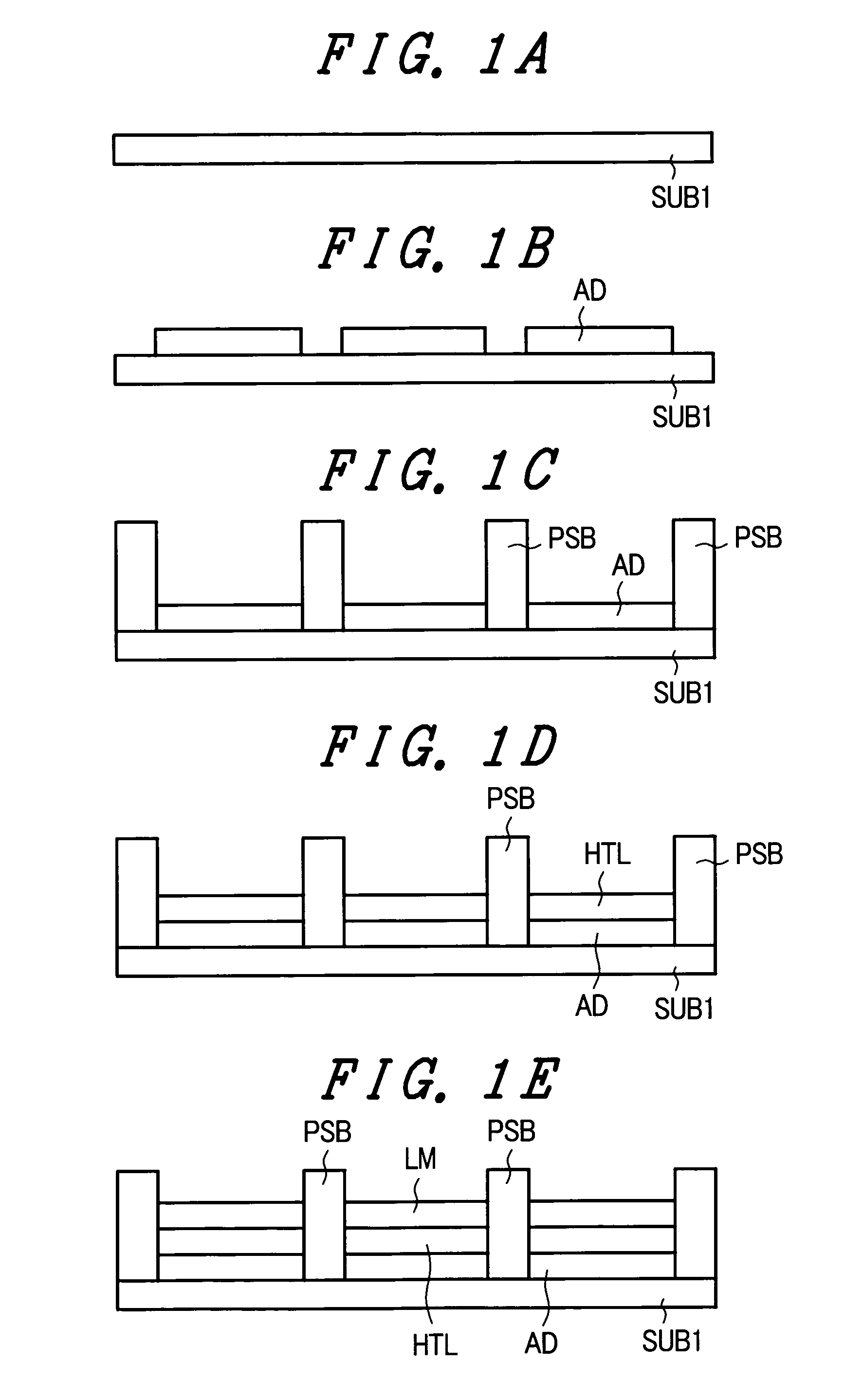
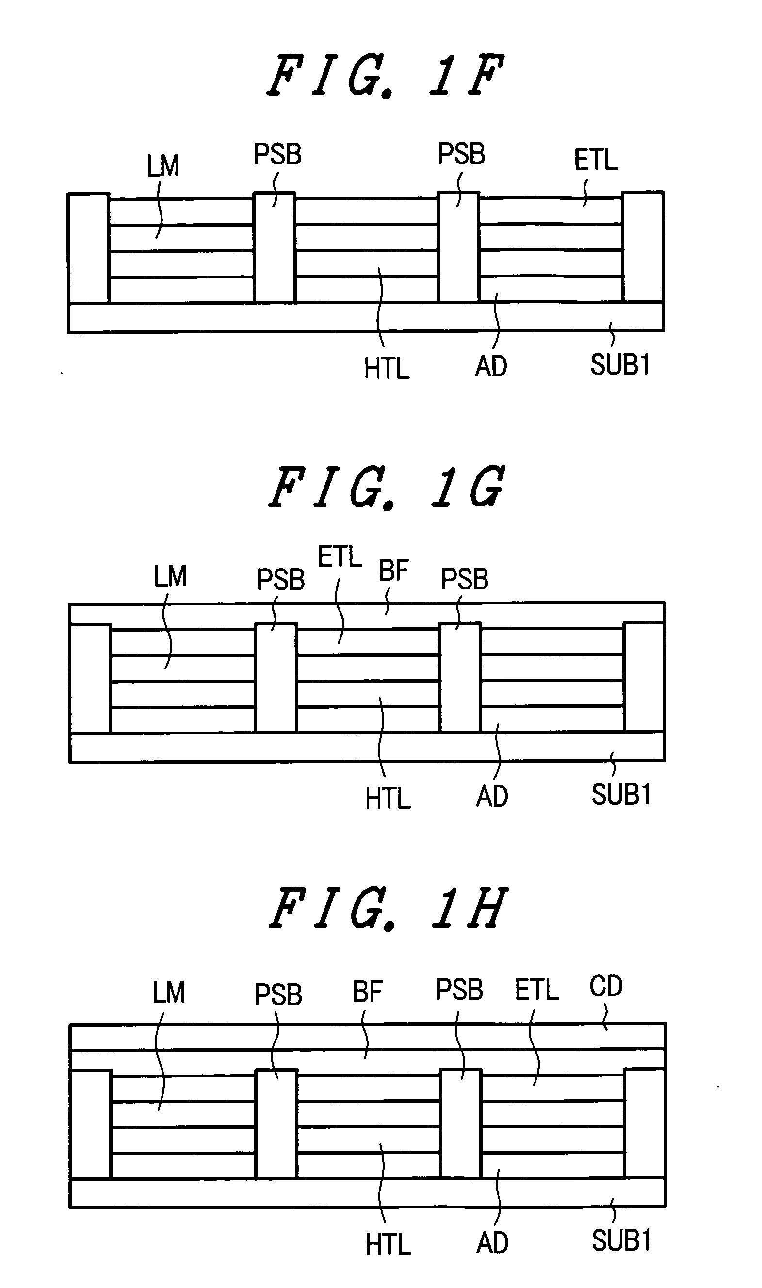
[0091]FIG. 1A and FIG. 1B show steps for explaining an embodiment 1 of a manufacturing method of an organic EL panel to which the present invention is applied. Steps advance in order of (a)→(b)→(c)→(d)→(e) in FIG. 1A and, thereafter, (f)→(g)→(h) in FIG. 1B. First of all, an ITO film having a thickness of 150 nm is formed by sputtering on a glass substrate SUB1 having a thickness of 1.1 mm on which thin film transistors are formed. Next, a portion of the ITO which is formed into the film is patterned by an etching treatment using a photolithography method thus forming anodes AD which constitute respective pixel portions. Here, the anodes AD are connected with source electrodes of thin film transistors via contact holes. Thin film transistors formed on the glass substrate SUB1 constitute driving transistors (second switches described later in FIG. 4).

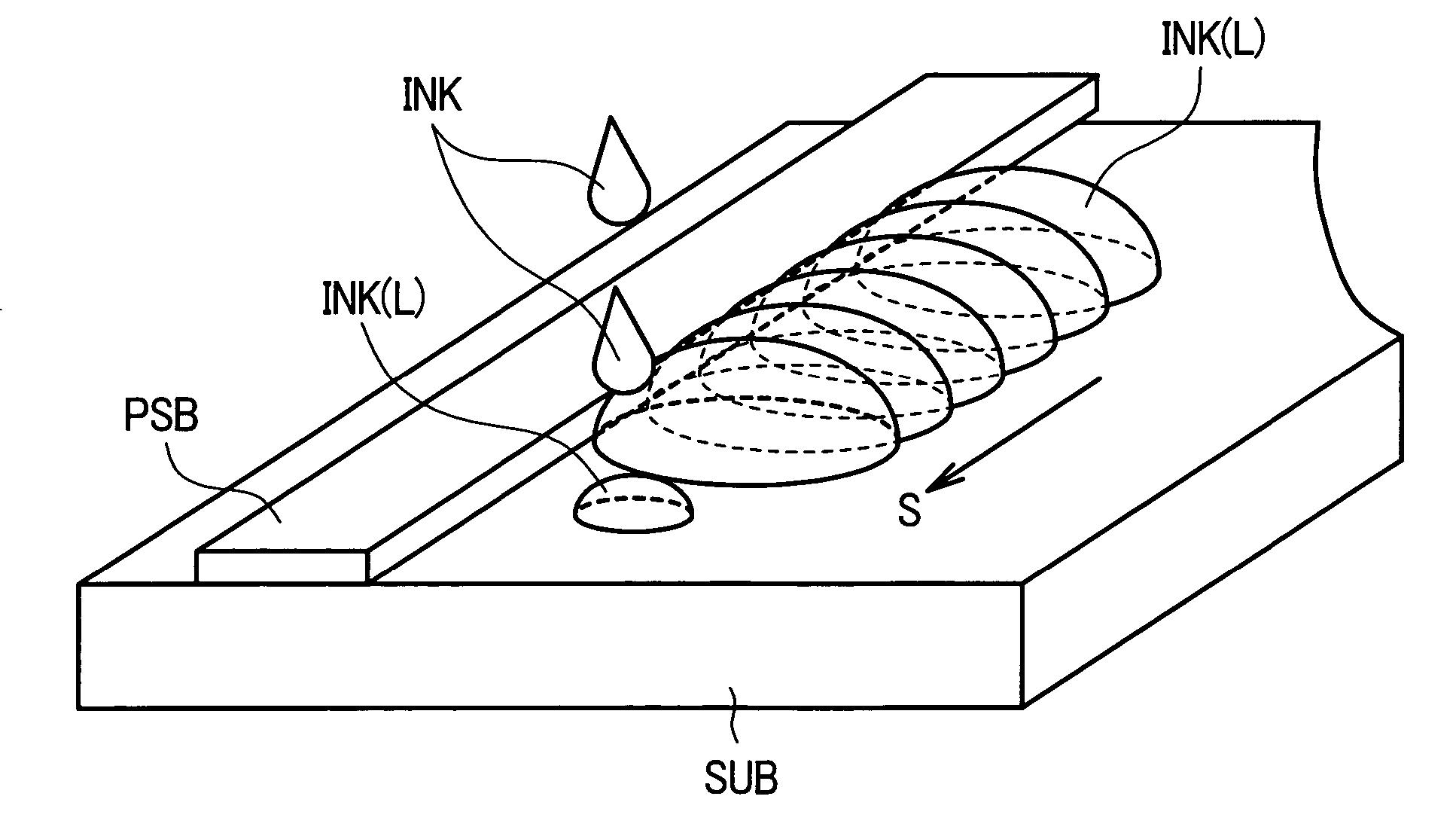
[0092] Subsequently, banks PSB having a film thickness of 2 μm which define pixel portions in a state that the banks PSB surround the p...

embodiment 2

[0105]FIG. 4 shows steps for explaining an embodiment of a manufacturing method of an organic thin film transistor to which the present invention is applied. First of all, to a polyimide substrate SUB1 having a thickness of 150 μm, Au having a thickness of 20 nm is vapor-deposited at a vapor deposition rate 0.1 nm / second under a vacuum of 10−6 torr. The vapor-deposited Au is patterned using a photolithography method thus forming source electrodes SD1 and drain electrodes SD2. A length of a channel between the source electrode SD1 and the drain electrode SD2 is set to 10 μm.

[0106] Next, 1,3,5-Tris[4-(diphenylamino)phenyl]-benzene (TDAPB, produced by Bayer Co.) is dissolved in a 1:1 mixed solvent of 1,2-dimethoxybenzene and cyclohexanol such that the concentration of solid content becomes 0.5 wt % thus forming organic-semiconductor-layer-forming ink through a PTFE filter of 0.2 μm. The ink is discharged using a nozzle of a piezoelectric ink jet device to form a film having a thicknes...


PUM


Abstract

The present invention provides a method which can form a uniform amorphous film using an organic low molecular weight material which is refined by distillation or sublimation. The viscosity of ink is regulated by mixing two kinds of solvents so as to increase a surface tension of the ink and the solubility of the organic material in a drying step whereby an amorphous film made of an organic material is selectively formed in a recessed region defined by a partition wall layer using an ink jet method.

Description

CROSS-REFERENCE TO RELATED APPLICATIONS [0001] The disclosure of Japanese Patent Application No. 2004-249050 filed on Aug. 27, 2004 including the specification, drawings and abstract is incorporated herein by reference in its entirety. BACKGROUND OF THE INVENTION [0002] 1. Field of the invention [0003] The present invention relates to a method for forming a constitutional layer of an electron device and a material thereof and, for example, a method for coating a light emitting layer of an organic EL panel, an electrode or a semiconductor layer of a semiconductor such as an organic thin film transistor using an ink jet method, and the ink composition which is preferably used for such coating. [0004] 2. Description of the Related Arts [0005] With respect to the a polymer electroluminescence panel (an organic EL display device, hereinafter simply referred to as an organic EL panel or an OLED) or various electron devices which include semiconductor elements such as thin film transistors...

Claims


Application Information

Patent Timeline
Patent Type & Authority Applications(United States)
IPC IPC(8): B05D5/06C09D11/00C09D11/322H01L21/288H01L21/336H01L29/786H01L51/05H01L51/40H01L51/50H05B33/10
CPCC09D11/30H01L27/3295H01L51/0005H01L51/0025H01L51/56H01L51/0059H01L51/007H01L51/0085H01L51/0037H10K71/135H10K59/122H10K71/311H10K85/1135H10K85/6565H10K85/631H10K85/342H10K71/00
Inventor YASUKAWA, AKIKOUCHINO, SHOICHIARAI, YOSHIHIROTANAKA, MASAHIROITO, MASATOYAGUCHI, TOMIO
Owner HITACHI DISPLAYS
Why Eureka
Try Eureka