Antireflection film

Inactive Publication Date: 2006-03-09
DAI NIPPON PRINTING CO LTD
View PDF8 Cites 58 Cited by
  • Summary
  • Abstract
  • Description
  • Claims
  • Application Information

AI Technical Summary

Benefits of technology

[0015] Accordingly, it is an object of the present invention to eliminate the drawbacks of the prior art, that is, low processing speed due to the necessity of a lot of time for the formation of the transparent

Problems solved by technology

The reflection of external light from the surface of displays, however, significantly lowers the visibility.
An attempt to form these layers, for example, by sputtering requires a lot of time which thus disadvantageously results in low processing speed.
In addition, transparent conductive thin layers formed of ITO or the like posses excellent transparency, but on the other hand, disadvantageously, the corrosion resistance is unsatisfactory.
Further, in the antireflection member having the above construction, the reflectance on red light side and blue light side in the visible light region (wavelength 450 nm to 650 nm), in which humans feels glaring, is not satisfactorily evenly lowered.
Further, the antireflection member cannot satisfactorily cope with scratch and stain caused at the time of handling

Method used


Image

  • Antireflection film
  • Antireflection film
  • Antireflection film

Examples


example 1

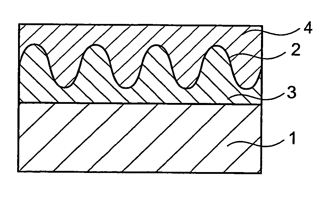
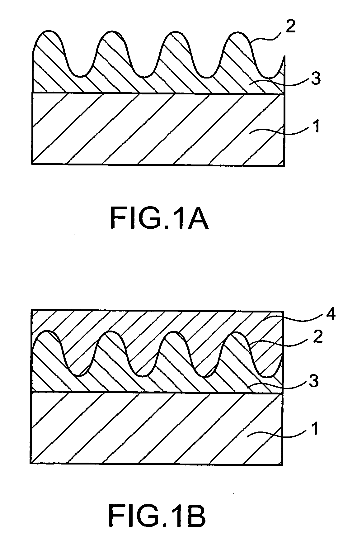
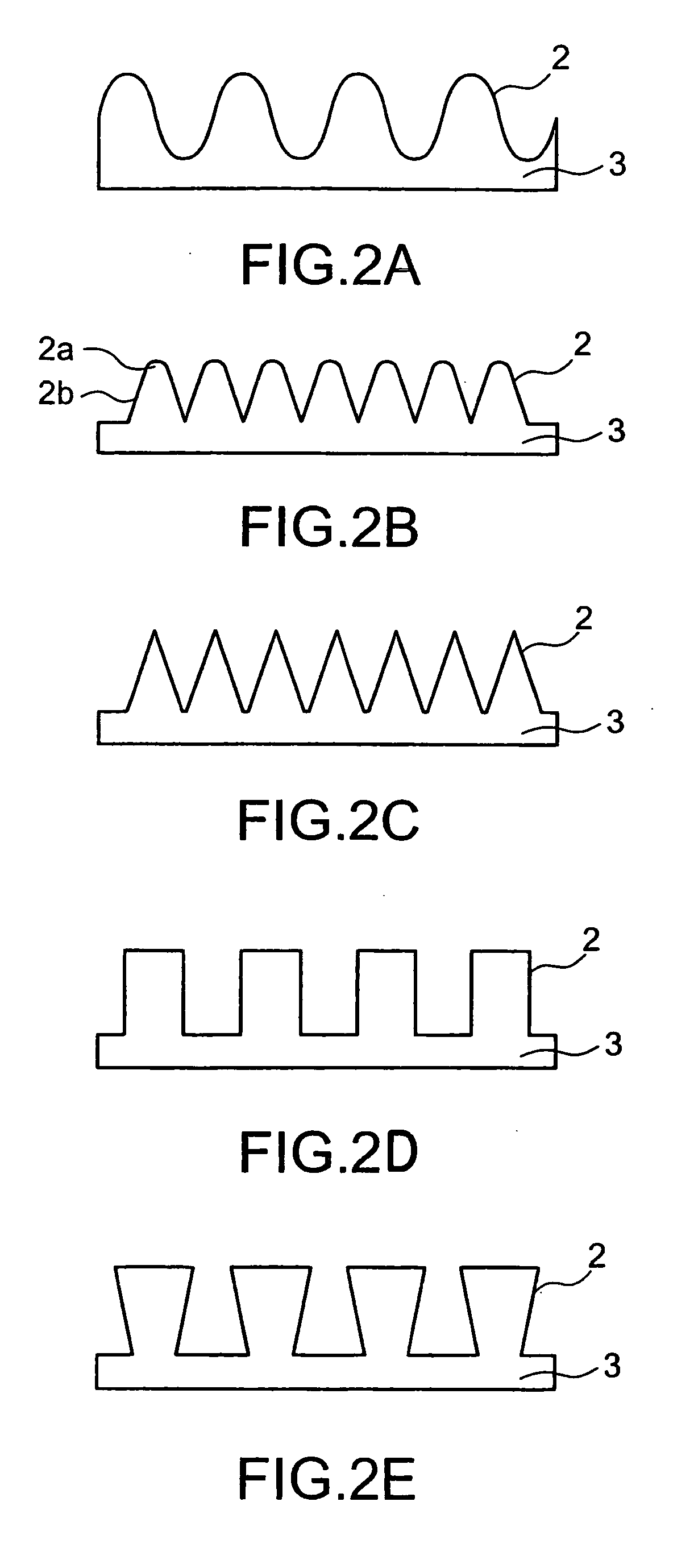
[0112] A photosensitive resin was coated by a spinner onto a glass substrate with a diameter of 76 mm to prepare a photosensitive material. The photosensitive material was exposed by means of a laser interference exposure system using an argon laser (wavelength 351 nm) at an angle of incidence of 40 degrees from three directions. After the exposure, solvent development was carried out to prepare an original mold having fine concaves and convexes arranged lengthwise and breadthwise on a cured product of the photosensitive resin.

[0113] The pitch of concaves and convexes on the original mold was 280 nm, and the difference in level between concaves and convexes was 200 to 250 nm.

[0114] The surface of the original mold was electrolessly plated, followed by plating with nickel to prepare a 100 μm-thick duplicate mold. This procedure was repeated to prepare duplicate molds. A large mold having a width of 500 mm and a length of 980 mm was prepared by multi-side attachment of the duplicate...

example 2

[0118] A fluororesin-based surface coating liquid was coated by dipping on fine concaves and convexes on the cured film in the antireflection film prepared in Example 1. The coating was then dried to prepare an antireflection film.

[0119] Fingerprints were applied onto the surface of this antireflection film, and the surface of the antireflection film was then wiped with cotton. As a result, the fingerprints could be wiped off.

example 3

[0120] An antireflection film was prepared in the same manner as in Example 1, except that a coating composition (an ATO ultrafine particles coating composition, manufactured by Shinto Paint Co., Ltd.) containing ultrafine particles of ATO (antimony-dopedindium tin oxide) was coated onto the easy-adhesion polyester resin film as used in Example 1.


PUM

PropertyMeasurementUnit
Electrical conductoraaaaaaaaaa
Transparencyaaaaaaaaaa
Refractive indexaaaaaaaaaa

Abstract

An object of the present invention is to eliminate drawbacks of conventional multi-layered antireflection films, that is, that a lot of time is required in the formation of a transparent conductive thin film and a low-refractive index layer leading to low processing speed, the corrosion resistance of the transparent conductive thin film is unsatisfactory, and the reflectance over the whole visible light region is not constant. This object can be attained by adopting a structure comprising: a transparent layer 3, with a pencil hardness of H or more, formed of a cured product of an ionizing radiation-curable resin composition; provided on one side of the transparent layer 3, a concave-convex portion 2 comprising innumerable fine concaves and convexes provided at a pitch of not more than the wavelength of light; a transparent substrate film 1 optionally provided on the transparent layer 3 on its side remote from the concave-convex portion 2; and a cover layer, having a lower refractive index than the transparent layer, preferably provided on the fine concaves and convexes.

Description

[0001] This is a Continuation of Application No. 09 / 804,081 filed Mar. 13, 2001. The entire disclosure of the prior application is hereby incorporated by reference in its entirety.TECHNICAL FIELD [0002] The present invention relates to an antireflection film which can prevent a lowering in visibility of various articles caused by the glare of light as a result of the reflection of light from the surface of the articles. [0003] The present invention also relates to an antireflection film which can develop antireflection properties by virtue of the adoption of a structure of fine concaves and convexes, at a pitch of not more than the wavelength of light, present on the surface thereof, and a polarizing element and a display device using the antireflection film. BACKGROUND OF THE INVENTION [0004] Liquid-crystal displays, CRT (cathode-ray tube) displays, plasma displays or other displays are required to have high visibility of images displayed on these displays. The reflection of extern...

Claims


Application Information

Patent Timeline
IPC IPC(8): G02B5/30G02B1/11G02B5/02G02B1/118G02B1/14G02B1/16G02B1/18G02F1/1335H01J29/89
CPCG02B1/11G02B1/118H01J2229/8915H01J29/896G02F1/133502Y10S359/90G02F2201/38G02F1/133528
Inventor ARAKAWA, FUMIHIROSUZUKI, HIROKO
Owner DAI NIPPON PRINTING CO LTD
Why Eureka
Try Eureka