Activation signal output circuit and determining circuit

a signal output circuit and signal output technology, applied in the direction of electronic switching, pulse technique, instruments, etc., can solve the problems of difficult suppression of power consumption during standby time difficult to achieve target lower power consumption, etc., to enhance detection sensitivity, sharply reduce erroneous detection, and improve performance

Inactive Publication Date: 2006-04-06
DENSO CORP
View PDF2 Cites 7 Cited by
  • Summary
  • Abstract
  • Description
  • Claims
  • Application Information

AI Technical Summary

Benefits of technology

[0075] Further, according to the twelfth invention of the present application, the binarization circuit can be configured at low power consumption, so that the start signal output circuit which is of low power consumption as the whole can also be realized. That is, according to the twelfth invention, the circuits preceding to the binarization circuit, such as the detection/amplification circuit, can be enhanced in performance by the configuration of the low power consumption, so that the CMOS circuit requiring the DC potential input of high level can also be employed for the succeeding binarization circuit.
[0076] Further, according to the thirteenth invention of the present application, in the determination circuit, it is permitted or facilitated that the relation between the magnitudes of the determination criterion potential and the detection potential, in two outputs which fluctuate in accordance with the existence or nonexistence of the arrival (detection) of radio frequency power, be greatly inverted on the basis of the existence or nonexistence. With such settings, accordingly, it is permitted or facilitated to enhance the detection sensitivity or to sharply decrease erroneous detection. Further, with such settings, it is permitted or facilitated to effectively suppress the number of transistors to be used and power consumption in the wh

Problems solved by technology

Under the premise of a battery operation or the like, however, lowering power consumption as desired is difficult when the operational amplifier requiring the current of mA order is adopted.
In such an apparatus, however, a signal generator, a LNA, a mixer, etc. must be always operated, and power consumption during a standby time period is therefore difficult to be suppressed.
Thus, the target lower power consumption is not attained, either.
On the other hand, the prior art sensing scheme based on the diode is difficult to enhance a sensing sensitivity.
These circumstances will be major causes for making difficult the compatibility between the higher sensitivity and lower power consumption of the wave-detector circuit.
As a result, the biases of the sensing diode and amplifier cannot be made independent.
On this occasion, however, unless the bias of the amplifier properly lowers in balanced fashion likewise to the bias of the diode detection circuit, the start signal output circuit 900 does not appropriately operate as a whole when the supply voltage Vcc lowers greatly.
That is, the circuit of the prior art arrangement (example: start signal output circuit 900 in FIG. 38), which does not have a flexible corresponding mechanism (balancing function) capable of coping with such a problem relevant to the lowering of the output voltage of the power supply, is apprehended to erroneously operate in some cases.
Further, in a high-temperature environment, thermal noise, flicker noise, etc. are liable to develop within a circuit as is often observed in case of using, for example, MOSFETs for the circuit.
As also seen from the foregoing circuit arrangement in FIG. 39B, the addition of such a determination circuit

Method used


Image

  • Activation signal output circuit and determining circuit
  • Activation signal output circuit and determining circuit
  • Activation signal output circuit and determining circuit

Examples


first embodiment

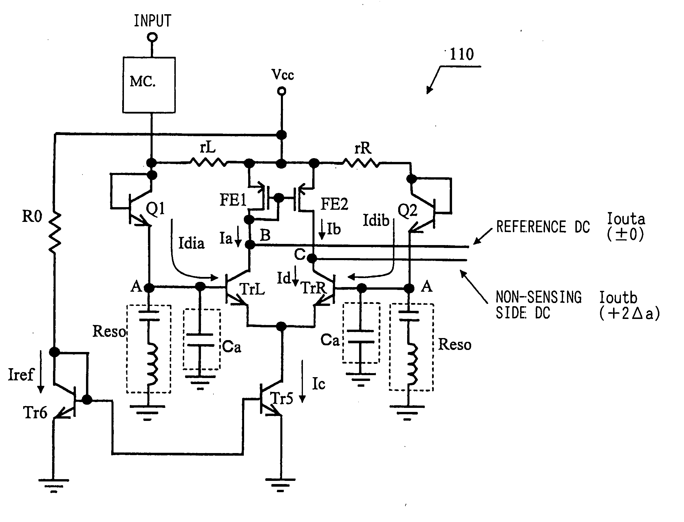
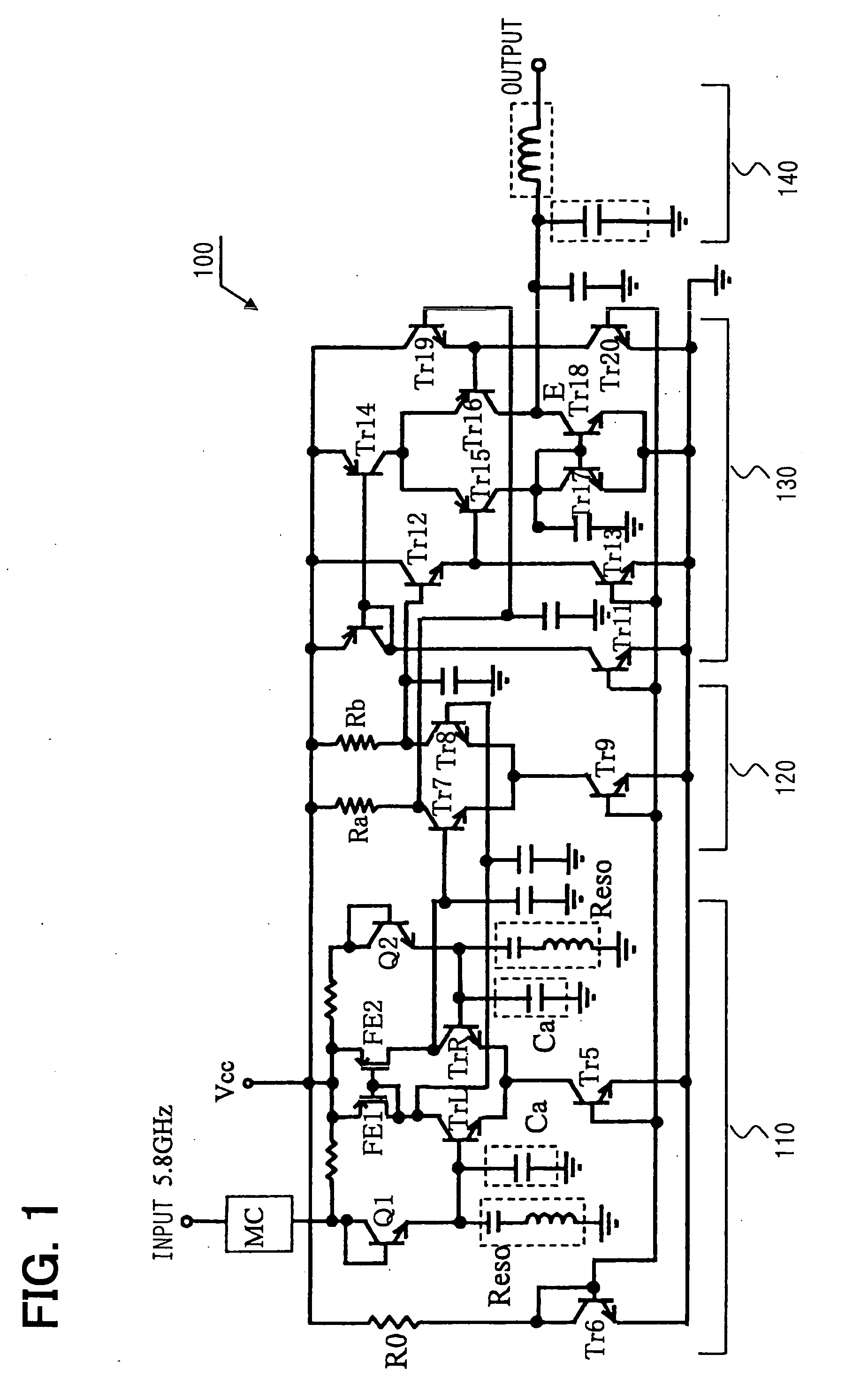
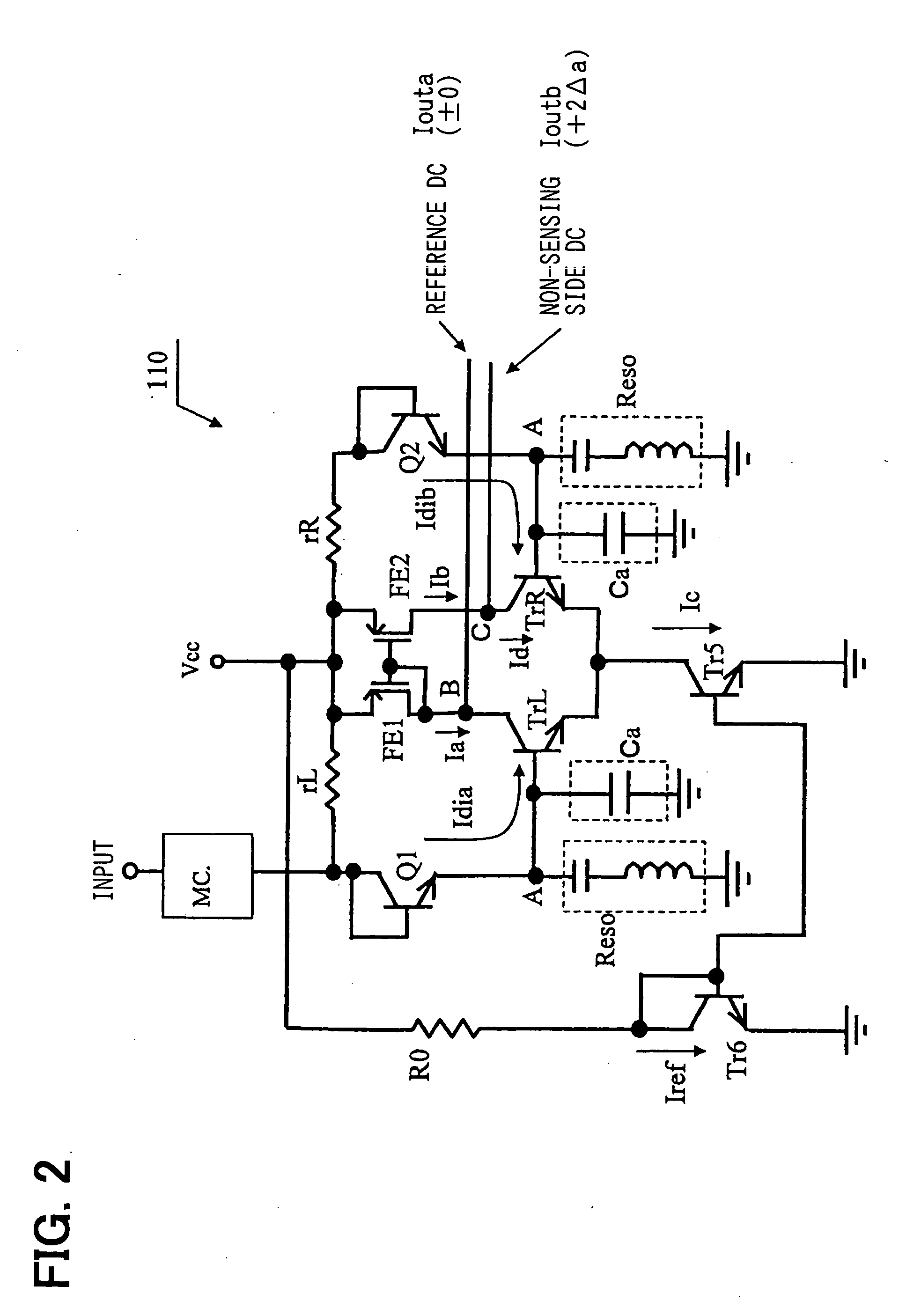
[0138]FIG. 1 is a circuit diagram of a start signal output circuit 100 in this embodiment. The start signal output circuit 100 includes an RF / DC conversion circuit to which radio frequency power (RF) of specified frequency is inputted and from which a direct current potential (DC) is outputted.

100>

[0139] In the start signal output circuit 100, input power (radio frequency) is first converted into a DC via a matching circuit, a sensing diode Q1 and a low-pass filter (Reso, Ca), and the DC is amplified by a transistor TrL of differential pair transistors, thereby to amplify the potential difference between the collector terminals of the differential pair transistors TrL and TrR. The potential of the base terminal of the transistor TrR is internally set by employing the fifth invention of the present application.

[0140] In a determination circuit 120 at a succeeding stage, a threshold value (offset) is set for the DC potential thus detected and amplified in and outputted from a detect...

second embodiment

[0188] The second embodiment exemplified in conjunction with the drawings of FIGS. 13 through 24 is in order to solve these problems. As means for solving the problems, by way of example, the foregoing embodiment is modified so that a voltage doubler wave-detector circuit can be utilized for the detection / amplification circuit, an S / N ratio is enhanced by employing MOSFETs of large gates, or it is permitted to obtain a large amplitude by introducing active loads configured of transistors, into the determination circuit. Further, a combination with a binarization circuit utilizing CMOS is considered so that the power consumption can be further lowered.

[Voltage Doubler Wave-Detector Circuit]

[0189]FIG. 13 is a circuit diagram exemplifying a start signal output circuit 200 in the second embodiment. Further, FIG. 14 is a circuit diagram of a detection / amplification circuit 210 which is included in the start signal output circuit 200. In the second embodiment, first of all, as shown in ...

third embodiment

[0226] As a method for attaining a large amplitude (gain) in the determination circuit (example: determination circuit 120 in FIG. 1), there is described, for example, the method in which the appropriate load resistors (ra, rb and rc) are employed as exemplified in detail in FIG. 3 in the foregoing first embodiment. Alternatively, however, there is a method in which the gain of the differential pair transistors of the differential amplifier of the determination circuit is enhanced. The method is, for example, one in which Darlington connection is employed for the part of the differential pair transistors of the differential amplifier of the determination circuit.

[0227]FIG. 25 exemplifies a determination circuit 222 in which the determination circuit 120 (FIG. 3) in the foregoing first embodiment is reconfigured using the Darlington connection. Incidentally, also here, load resistors are set at Ra


PUM


Abstract

A start signal output circuit having an RF/DC conversion circuit to which radio frequency power (RF) of specified frequency is inputted and from which a direct current potential (DC) is outputted, comprises a detection/amplification circuit 210 which includes a voltage doubler wave-detector circuit 10 configured including a sensing diode Q1 (Tr34) for sensing the RF power, a differential amplifier including differential pair transistors Tr31 and Tr32, and a current mirror circuit. A base current of one Tr31 of the differential pair transistors is brought into substantial agreement with a DC component of a current flowing through the sensing diode Q1 (Tr34). A total of currents flowing through the differential pair transistors Tr31 and Tr32 is regulated to a substantially constant value by the current mirror circuit. Thus, the start signal output circuit which is small in size, high in sensitivity and low in power consumption can be realized.

Description

TECHNICAL FIELD [0001] The present invention relates to a start signal output circuit having an RF / DC conversion circuit, which inputs radio frequency power (RF) of specified frequency and outputs direct current potential (DC), and a determination circuit very useful for the start signal output circuit and the like. [0002] Herein, the direct current potential (DC) signifies an output potential which is generated on the basis of a detection potential from a sensing diode as developing during a time period for which the level (amplitude) of a waveform determined by the envelope of the waveform of the radio frequency power (RF) has a substantially constant value or above. [0003] Accordingly, in a case where the RF power (RF) arrives intermittently or where the arrival is periodic, the waveform of the DC potential (DC) can become periodic. Even in a case, for example, where the DC potential (DC) fluctuates periodically or intermittently in such a manner, the present invention is, of cou...

Claims


Application Information

Patent Timeline
IPC IPC(8): G01R25/00H03F3/45H03D1/10H03D1/18H03F3/68
CPCH03D1/10H03D1/18
Inventor MIZUNO, KAZUOKIMURA, RYUKAGO, YOSHIYUKITANAKA, YUKIOMIENDO, KAZUHIKOUDA, HISANORIHAYASHI, HIROAKI
Owner DENSO CORP
Why Eureka
Try Eureka