Method for forming an electrode

a technology of electrodes and electrodes, applied in the direction of photovoltaic energy generation, electrical equipment, semiconductor devices, etc., to achieve the effects of high light-transmittivity, low resistivity, and high transparency

Active Publication Date: 2006-04-06
TOYODA GOSEI CO LTD
View PDF4 Cites 27 Cited by
  • Summary
  • Abstract
  • Description
  • Claims
  • Application Information

AI Technical Summary

Benefits of technology

[0012] Effects to be obtained by the present invention are explained as follows.
[0013] As described below, the inventors of the present invention invented to form the optimum light-transparent electrode by depositing ITO through electron beam deposition or ion plating treatment in the low pressure oxygen ambient. The inventors of the present invention also invented that an electrode having high light-transmittivity and low resistivity can be obtained by heating to bake the ITO after that deposition treatment. The inventors of the present invention further invented that an electrode having high transparency and low resistivity can be obtained by not carrying out baking when the ITO is formed in the oxygen ambient of 0.06 Pa or more.
[0014] A pad electrode for wire bonding which contacts to the light-transparent electrode made of ITO needs to be formed, but the inventors of the present invention found that adhesiveness of the ITO electrode can be improved by forming at least one of nickel (Ni), titanium (Ti), chromium (Cr), and aluminum (Al) between a thick film electrode made of Au and ITO electrode.

Problems solved by technology

With respect to indium tin oxide (ITO), however, its characteristic is not yet found out when it is employed in a Group III nitride compound semiconductor light-emitting device, and it needs to develop the optimum condition for forming an electrode by using indium tin oxide (ITO).

Method used


Image

  • Method for forming an electrode
  • Method for forming an electrode

Examples


embodiment 1

[0027] First, the inventors of the present invention carried out the following experiment to show that desired improvement of luminous transparency of the ITO and decrease of sheet resistivity can be obtained by employing a method for forming an electrode according to the present invention. By using a mixture of tin oxide (5%) and indium oxide as a target, 300 nm in thickness of ITO was formed on a sapphire substrate through electron beam deposition. After the atmosphere in the deposition chamber was arranged to be high vacuum of 1×10⁻² Pa or less, oxygen was supplied at 4 different pressures to obtain each ITO. 5 oxygen pressures were: 0.0 Pa (without supplying oxygen), 0.005 Pa, 0.015 Pa, 0.06 Pa, and 0.1 Pa. After forming 4 types of ITO, luminous transparency for blue-color light having wavelength of 470 nm and sheet resistivity were measured. Then each of the ITO was heated for 10 minutes in the nitrogen ambient at the temperature of 400° C., and luminous transparency and sheet ...

embodiment 2

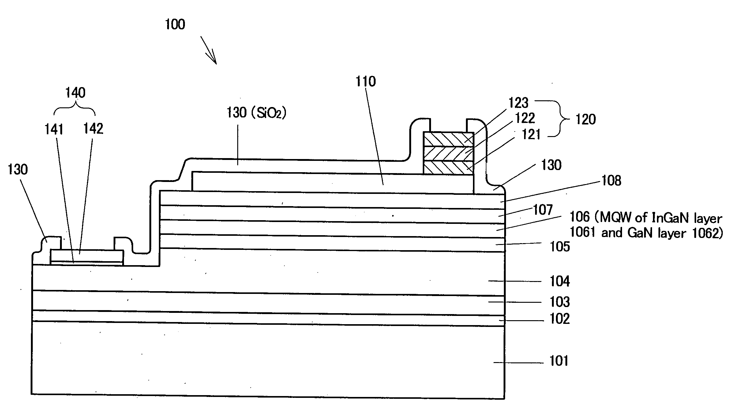
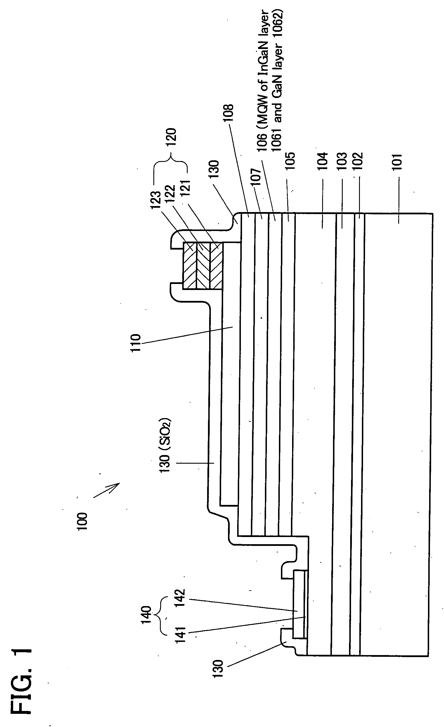
[0034]FIG. 1 illustrates a sectional view of a semiconductor light-emitting device 100 according to the second embodiment of the present invention. As shown in FIG. 1, the semiconductor light-emitting device 100 comprises about 300 μm in thickness of sapphire substrate 101, on which about 15 nm in thickness of aluminum nitride (AlN) buffer layer 102, about 500 nm in thickness of undoped GaN layer 103, and about 5 μm in thickness of silicon (Si) doped GaN n-type contact layer 104 (high carrier concentration n+-layer) having Si concentration of 1×10¹⁸ / cm3 are deposited.

[0035] On the n-type contact layer 104, about 25 nm in thickness of silicon (Si) doped n-type Al0.15Ga0.85N n-type layer 105 having Si concentration of 1×10¹⁷ / cm3 is deposited, and an emission layer 106, which has multiple quantum-well structure and comprises 3 pairs of about 3 nm in thickness of undoped In0.2Ga0.8N well layer 1061 and about 20 nm in thickness of undoped GaN barrier layer 1062, is formed thereon.

[0036...


PUM


Abstract

In a semiconductor light-emitting device 100, a buffer layer 102, a undoped GaN layer 103, a high carrier concentration n+-layer 104, an n-type layer 105, an emission layer 106, a p-type layer 107, and a p-type contact layer 108 are deposited in sequence on a sapphire substrate. The semiconductor light-emitting device 100 comprises a light-transparent electrode 110 made of indium tin oxide (ITO) which is deposited in the low pressure vacuum chamber flowing at least oxygen gas through electron beam deposition or ion plating treatment and thermal process are carried out.

Description

[0001] This is a patent application based on a Japanese patent application No. 2004-288974 which was filed on Sep. 30, 2004, and which is incorporated herein by reference. TECHNICAL FIELD [0002] The present invention relates to a method for forming an electrode of a semiconductor device which is formed by depositing a Group III nitride compound semiconductor. Especially, the present invention relates to a light-transparent electrode, i.e., luminous transparent electrode, made of indium tin oxide (ITO). BACKGROUND ART [0003] Presently, a Group III nitride compound semiconductor device is generally grown on a non-conductive sapphire substrate, and comprises an n-electrode and a p-electrode both of which are formed at a semiconductor device layer side. Here, a lateral type of Group III nitride compound semiconductor device has a thin-film light-transparent electrode made of, for example, an alloyed gold (Au) and cobalt (Co) on the surface of a p-type layer, and outputs lights from the ...

Claims


Application Information

Patent Timeline
Patent Type & Authority Applications(United States)
IPC IPC(8): H01L21/28H01L21/44H01L33/06H01L33/12H01L33/32H01L33/42
CPCH01L24/03H01L2224/02166H01L24/06H01L31/1884H01L33/42H01L2224/05073H01L2224/05082H01L2224/05644H01L2924/01004H01L2924/01005H01L2924/01007H01L2924/01012H01L2924/01013H01L2924/01014H01L2924/01015H01L2924/01016H01L2924/0102H01L2924/01022H01L2924/01025H01L2924/01027H01L2924/01028H01L2924/0103H01L2924/01032H01L2924/01033H01L2924/01038H01L2924/01047H01L2924/01049H01L2924/0105H01L2924/01051H01L2924/01052H01L2924/01056H01L2924/01078H01L2924/01079H01L2924/01082Y02E10/50H01L24/05H01L2924/12041H01L2924/01006H01L2924/01023H01L2924/01024H01L2924/00014
Inventor YOSHIDA, KAZUHIROHASEGAWA, YUKITAKAKAGA, KOJI
Owner TOYODA GOSEI CO LTD
Why Eureka
Try Eureka