Capacitance multiplier circuit exhibiting improved bandwidth

a multiplier circuit and capacitor technology, applied in the direction of pulse technique, process and machine control, instruments, etc., can solve the problems of reduced convenience at the application level, increased pin-out cost, and substantial die area incurred in the construction of these capacitors, so as to reduce the series resistance of the current sensing path, increase bandwidth, and reduce the effect of cos

Inactive Publication Date: 2006-04-27
ASAHI KASEI TOKO POWER DEVICE
View PDF5 Cites 5 Cited by
  • Summary
  • Abstract
  • Description
  • Claims
  • Application Information

AI Technical Summary

Benefits of technology

[0007] By contrast, the present invention employs a cascoded current summing topology, in which a capacitive current is summed into a virtual node formed by the source-drain connection of two transistors. This arrangement reduces the series resistance of the current sensing path. As a consequence, the present multiplier circuit remains capacitive at higher frequencies than are possible using prior art mirror approaches. This attribute is beneficial to the performance of filters and compensator networks in which the capacitance multiplier may be used. In particular, the resulting higher bandwidth permits greater design flexibility since the zero frequency has been pushed higher, often outside of the critical range.

Problems solved by technology

Unfortunately, a substantial die area may be incurred in the construction of these capacitors.
Alternatively, larger capacitors may also be placed external to the die, but at the expense of a pin-out increase and reduced convenience at the application level.
In terms of frequency response, the known mirror-based approaches have a bandwidth limit imposed by the series resistance of the sensing path.
At high frequencies, this limit causes the circuit to appear to be resistive rather than to exhibit the desired capacitive behavior.
Hence, the range and performance of filter and compensator networks using these multipliers may very well be limited.
This arrangement reduces the series resistance of the current sensing path.

Method used


Image

  • Capacitance multiplier circuit exhibiting improved bandwidth
  • Capacitance multiplier circuit exhibiting improved bandwidth
  • Capacitance multiplier circuit exhibiting improved bandwidth

Examples


Embodiment Construction

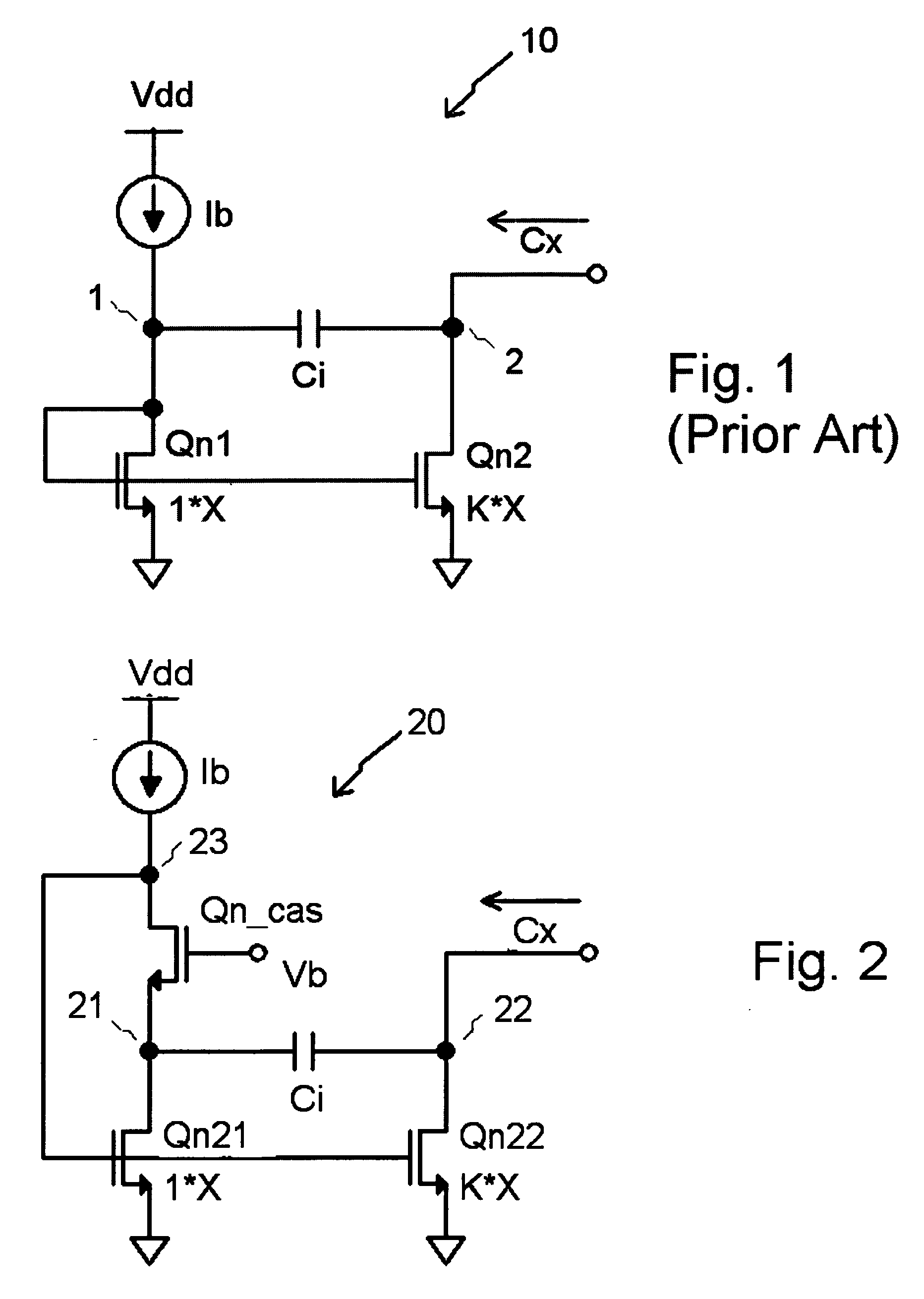
[0017] Referring first to FIG. 1, there is shown a prior art capacitance multiplier circuit 10. This circuit is biased by current source Ib. The direct current from source Ib flows through a diode-connected transistor Qn1, thereby establishing an operating voltage at node 1. The drain terminal of transistor Qn2 is biased such that Qn2 operates in the pinch-off region. The factor K represents the size ratio of Qn2 to Qn1. K is usually assumed to be a positive number greater than unity.

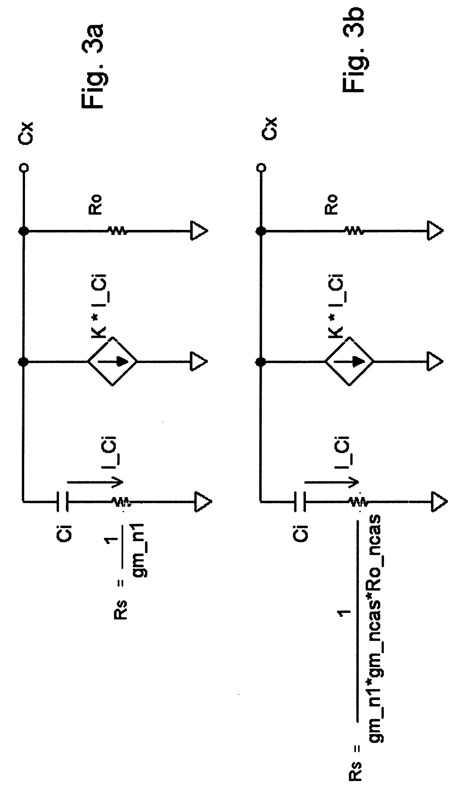
[0018] With these operating conditions established on devices Qn1 and Qn2, the small signal model shown in FIG. 3a can be applied to evaluate the bandwidth performance of the circuit 10. It should be noted that I_Ci represents the current in capacitor Ci.

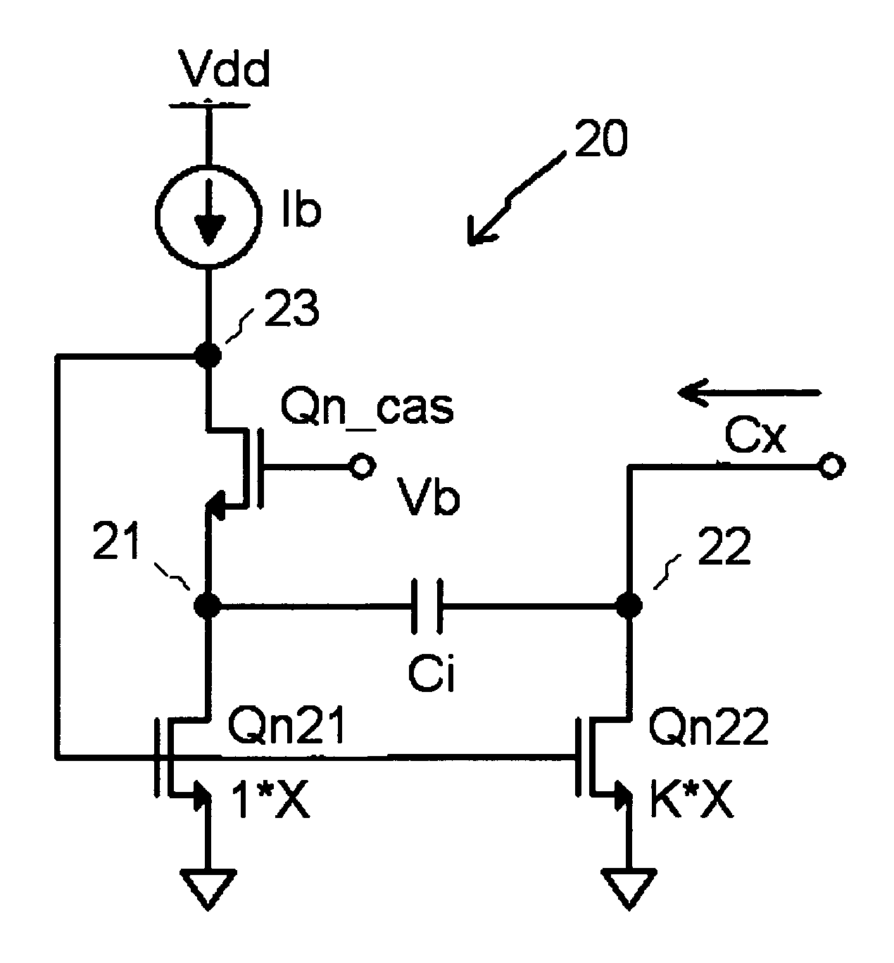
[0019] Referring now to FIG. 2, there is shown a detailed schematic diagram of a capacitance multiplier circuit 20 in accordance with the present invention. This circuit is biased by a current source Ib. The direct current from source Ib flows through...


PUM


Abstract

A monolithic capacitance multiplication circuit serves to reduce the required die area when larger capacitance values are needed such as in filter and loop frequency compensation circuits. A current mirror/cascoding device arrangement reduces the effective series resistance of the multiplier capacitor. As a result, the multiplier topology exhibits improved bandwidth over prior art capacitance multiplier circuits.

Description

BACKGROUND AND SUMMARY OF THE INVENTION [0001] The present invention relates to monolithic circuit topologies which function to magnify the apparent size of a capacitor that is used in a AC filtering or compensation applications. [0002] In integrated circuit designs, there is occasionally the need to use a relatively large capacitance to achieve the desired circuit performance. For example, to stabilize the feedback loop found in a phase lock loop or in a linear switch-mode voltage regulator, a low frequency zero can be installed in the loop gain to enhance the phase margin and improve transient response. Larger capacitance values on the order of tens of picofarads or more may be required, depending on the particular loop crossover frequency and circuit impedance levels. [0003] Unfortunately, a substantial die area may be incurred in the construction of these capacitors. In particular, in some 0.6 uM CMOS processes, a poly-poly capacitor may require about 800 μM2 per picofarad of ca...

Claims


Application Information

Patent Timeline
Patent Type & Authority Applications(United States)
IPC IPC(8): H03K19/094
CPCH03H11/405
Inventor SCHOENBAUER, STEVE
Owner ASAHI KASEI TOKO POWER DEVICE
Why Eureka
Try Eureka