Solid phase epitaxy recrystallization by laser annealing

a laser annealing and solid phase technology, applied in the field of solid phase epitaxy recrystallization by laser annealing, can solve the problems of increasing the difficulty of proportionally scaling down the depth and gradient of source/drain extension regions, undetected degradation of the operating parameters of the mos device, and significant short channel effects, etc., to achieve the effect of reducing sheet resistance, reducing activation levels and doping concentrations

Active Publication Date: 2006-04-27
TEXAS INSTR INC
View PDF2 Cites 24 Cited by
  • Summary
  • Abstract
  • Description
  • Claims
  • Application Information

AI Technical Summary

Benefits of technology

[0022] In the past, solid phase epitaxy has been carried out at low temperatures (e.g., <600° C.), leaving behind considerable end of range damage, including clusters of interstitial Si atoms. Subsequent attempts to anneal out this damage using conventional anneal apparatus has resulted in profile degradation, wherein the profile is less abrupt than that which may be achieved in the present invention. In addition, some aspects of the present invention have further been found to provide significant improvement in reducing sheet resistance compared with prior methods, such as illustrated in prior art FIG. 1 above. The processes, moreover, may advantageously achieve higher activation levels and doping concentrations throughout substantially all of the drain extension region adjacent the channel region than that of some prior art technologies.
[0023] Th

Problems solved by technology

As device sizes continue to shrink, the physical and effective channel lengths continue to be scaled downward, wherein short channel effects become significant.
The injected hot carriers, in turn, often lead to undesired degradation of the MOS device operating parameters, such as a shift in threshold voltage, changed transconductance, changed drive current/drain current exchange, and device instability.
As CMOS devices are scaled down to support future technologies, it has become increasingly problemat

Method used


Image

  • Solid phase epitaxy recrystallization by laser annealing
  • Solid phase epitaxy recrystallization by laser annealing
  • Solid phase epitaxy recrystallization by laser annealing

Examples


Embodiment Construction

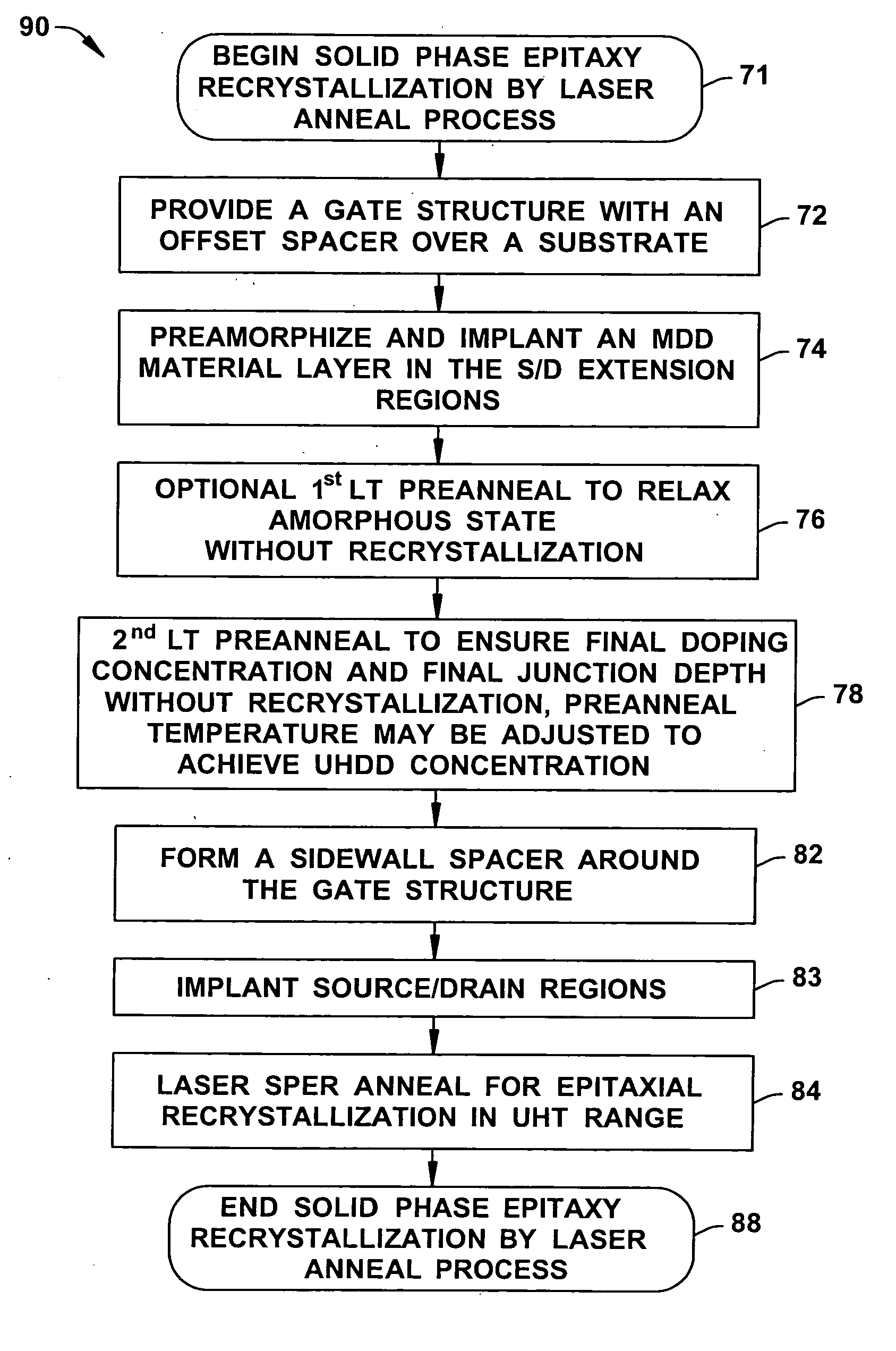
[0037] The present invention will now be described with reference to the attached drawings, wherein like reference numerals are used to refer to like elements throughout. The invention provides new processes for forming drain extension regions in the manufacture of transistor devices, wherein a deep preamorphized region is produced in the drain extensions, which are implanted with a dopant exhibiting an enhanced diffusion property in the amorphous phase. The dopant is then pre-annealed to set the junction depth, and laser annealed to facilitate a higher activation level and an abrupt gradient profile for shallow junction depths. Exemplary implementations are hereinafter illustrated and described in the context of fabricating pMOS transistors with a B or BF2 drain extension dopant implantation and anneal, wherein the structures illustrated are not necessarily drawn to scale. However, it will be appreciated that the invention may be employed separately or in combination in forming dra...


PUM


Abstract

Methods (70) are described for fabricating shallow and abrupt gradient drain extensions for MOS type transistors, in which a solid phase epitaxial recrystallization is performed within the drain extensions utilizing a laser SPER annealing process in the manufacture of semiconductor products. One method (70) includes a preamorphizing process (74) of implanting a heavy ion species such as Germanium deep into an extension region of a substrate adjacent a channel region of the substrate to form a deep amorphized region, then implanting boron or another such dopant species into an extension region of the substrate adjacent the channel region. The implanted dopant is then preannealed (78) at a low temperature to set the junction depth and doping concentration. The extensions and/or the deep source/drain regions are subsequently annealed (84) with a laser at a high temperature providing a solid phase epitaxial recrystallization in the regions proximate the channel region to achieve ultra high doping concentrations and activation levels with an abrupt gradient.

Description

FIELD OF INVENTION [0001] The present invention relates generally to semiconductor devices and more particularly to methods for performing a solid phase epitaxial recrystallization of the source and drain extensions of a transistor utilizing a laser annealing process in the manufacture of semiconductor products. BACKGROUND OF THE INVENTION [0002] MOS transistors are found in many modern semiconductor products where switching and / or amplification functions are needed. Many manufacturing processes and techniques have been developed for fabricating MOS devices in semiconductor substrate materials such as silicon and the like. In recent years, the size of transistors and other components have steadily decreased to submicron levels in order to facilitate higher device densities in semiconductor products. At the same time, many new applications have created a need to operate transistors and other semiconductor devices at lower power and voltage levels. Thus, whereas previous MOSFET device...

Claims


Application Information

Patent Timeline
IPC IPC(8): H01L21/336
CPCH01L21/26506H01L21/268H01L29/6656H01L29/6659H01L29/7833H01L21/2658H01L21/26513
Inventor JAIN, AMITABH
Owner TEXAS INSTR INC
Why Eureka
Try Eureka