Copper alloy thin films, copper alloy sputtering targets and flat panel displays

a technology of copper alloy and sputtering target, which is applied in the direction of discharge tube luminescnet screen, instrument, and semiconductor/solid-state device details, etc., can solve the problems of poor adhesion with glass substrate, insulation failure, and reduce the reliability of interconnection, so as to achieve satisfactory reliability and lower electrical resistivities

Inactive Publication Date: 2006-05-04
KOBE STEEL LTD
View PDF7 Cites 65 Cited by
  • Summary
  • Abstract
  • Description
  • Claims
  • Application Information

AI Technical Summary

Benefits of technology

[0009] Under these circumstances, an object of the present invention is to provide a Cu alloy thin film that can maintain a lower electrical resistivity than pure Al and inhibit void formation even after exposure to high temperatures in a fabrication process typically of flat panel displays. Another object of the present invention is to provide a sputtering target for depositing the Cu alloy thin film, and a flat panel display using the Cu alloy thin film as an interconnection film and / or electrode film.
[0014] The Cu alloy thin films are most suitable as interconnection films and / or electrode films for flat panel displays. Even after heat treatment at 200° C. to 500° C. for 1 to 120 minutes, Fe2P, Co2P, and Mg3P2 are precipitated at grain boundaries in the Cu alloy thin films (a), (b) and (c), respectively, to serve to maintain their low electrical resistivities and inhibit the formation of voids.
[0019] The Cu alloy thin films according to the present invention can yield Cu alloy interconnection films that maintain lower electrical resistivities than pure Al thin film and have satisfactory reliability without causing a large number of voids, even after being subjected to heat treatment at 200° C. or higher for the deposition of a gate insulator film and / or an interlayer dielectric film. The resulting interconnection films and / or electrode films are used for upsized flat panel displays such as liquid crystal displays, plasma display panels, field emission displays and electroluminescence displays.

Problems solved by technology

Upon application to liquid crystal displays, Ag, however, is poor in adhesion with glass substrates and / or SiN dielectric films, is not sufficiently processed into interconnections by wet etching and causes insulation failure due to the cohesion of the Ag element.
The tensile stress causes fine fractures called voids at grain boundaries in the metal interconnections, which in turn reduces the reliability of the interconnections, such as resistance to break caused by stress migration (SM resistance) or resistance to break caused by electromigration (EM resistance).
Thus, polycrystalline Cu interconnections suffer very large strain between different crystal orientations upon temperature fall after the heat treatment, which frequently causes grain boundary delamination (voids or cracks).
In addition, Cu is susceptible to oxidation, and internal oxidation and grain boundary delamination (voids or cracks) accompanied with this must be inhibited when Cu is used as a material for interconnections.
The grain boundaries include a large quantity of crystal defects of atomic vacancy, called “vacancy”, and this causes acceleration of oxidation.
In addition to the increased electrical resistance, the internal oxidation with grain boundary delamination significantly adversely affects the reliability of the interconnections, since it causes, for example, break of the interconnections.

Method used


Image

  • Copper alloy thin films, copper alloy sputtering targets and flat panel displays
  • Copper alloy thin films, copper alloy sputtering targets and flat panel displays
  • Copper alloy thin films, copper alloy sputtering targets and flat panel displays

Examples


example 1

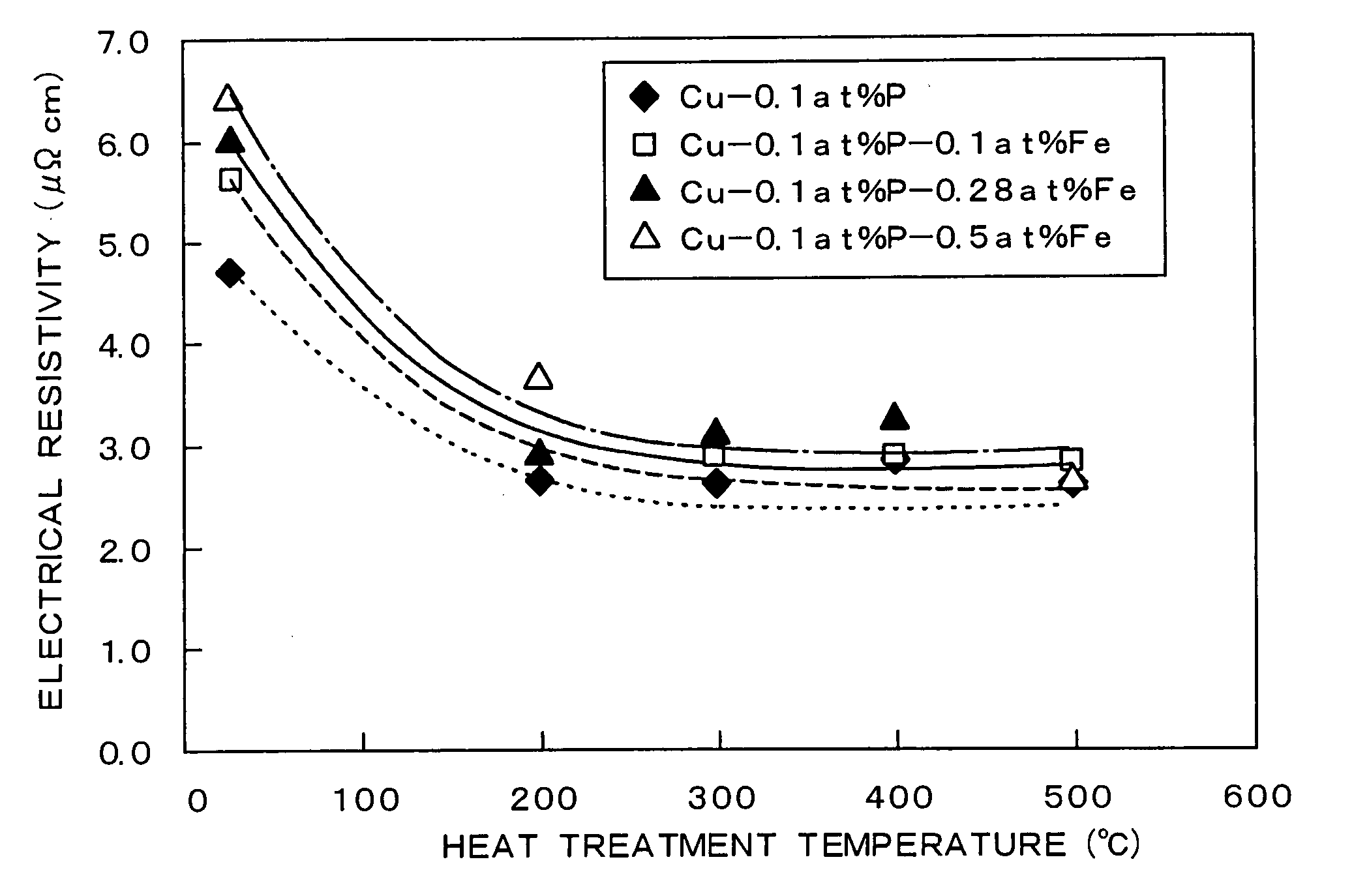
[0074] A sputtering target comprising a Cu alloy containing 0.28 atomic percent of Fe and 0.25 atomic percent of P with the balance being Cu and inevitable impurities was prepared by vacuum melting process. Using the sputtering target, a Cu—P—Fe alloy thin film having a thickness of 300 nm was deposited on a glass substrate (#1737 glass available from Corning Inc.) having a diameter of 50.8 mm and a thickness of 0.7 mm by DC magnetron sputtering. The composition of the Cu—P—Fe alloy thin film was analyzed by inductively coupled plasma (ICP) atomic emission spectrometry to find that the content of Fe is 0.28 atomic percent and that the content of P is 0.05 atomic percent. Upon film deposition, about 80% of P was not probably yielded due to its high vapor pressure.

[0075] Next, a positive-type photoresist (thickness of 1 μm) was patterned on the Cu-0.28 atomic percent Fe-0.05 atomic percent P alloy thin film, was etched with a mixed acid etchant, and the photoresist was removed with a...

example 2

[0077] A sputtering target comprising a Cu alloy containing 0.35 atomic percent of Co and 0.25 atomic percent of P with the balance being Cu and inevitable impurities was prepared by vacuum melting process. Using the sputtering target, a Cu—Co—P alloy thin film having a thickness of 300 nm was deposited on a glass substrate (#1737 glass available from Corning Inc.) having a diameter of 50.8 mm and a thickness of 0.7 mm by DC magnetron sputtering. The composition of the Cu—Co—P alloy thin film was analyzed by inductively coupled plasma (ICP) atomic emission spectrometry to find that the content of Co is 0.35 atomic percent and that the content of P is 0.05 atomic percent. Upon film deposition, about 80% of P was not probably yielded due to its high vapor pressure as in Example 1.

[0078] Next, a positive-type photoresist (thickness of 1 μm) was patterned on the Cu-0.35 atomic percent Co-0.05 atomic percent P alloy thin film, was etched with a mixed acid etchant, and the photoresist wa...

example 3

[0080] A sputtering target comprising a Cu alloy containing 0.5 atomic percent of Mg and 0.25 atomic percent of P with the balance being Cu and inevitable impurities was prepared by vacuum melting process. Using the sputtering target, a Cu—Mg—P alloy thin film having a thickness of 300 nm was deposited on a glass substrate (#1737 glass available from Corning Inc.) having a diameter of 50.8 mm and a thickness of 0.7 mm by DC magnetron sputtering. The composition of the Cu—Mg—P alloy thin film was analyzed by inductively coupled plasma (ICP) atomic emission spectrometry to find that the Mg content is 0.5 atomic percent and that the content of P is 0.05 atomic percent. Upon film deposition, about 80% of P was not probably yielded due to its high vapor pressure, as in Examples 1 and 2.

[0081] Next, a positive-type photoresist (thickness of 1 μm) was patterned on the Cu-0.5 atomic percent Mg-0.05 atomic percent P alloy thin film, was etched with a mixed acid etchant, and the photoresist ...


PUM

PropertyMeasurementUnit
resistivityaaaaaaaaaa
temperaturesaaaaaaaaaa
thicknessaaaaaaaaaa

Abstract

A Cu alloy thin film contains Fe and P with the balance being substantially Cu, in which the contents of Fe and P satisfy all the following conditions (1) to (3), and in which Fe2P is precipitated at grain boundaries of Cu after heat treatment at 200° C. to 500° C. for 1 to 120 minutes: 1.4NFe+8NP<1.3  (1)NFe+48NP>1.0  (2)12NFe+NP>0.5  (3)wherein NFe represents the content of Fe (atomic percent); and NP represents the content of P (atomic percent).

Description

BACKGROUND OF THE INVENTION [0001] 1. Field of the Invention [0002] The present invention relates to Cu alloy thin films, Cu alloy sputtering targets and flat panel displays. Specifically, it relates to Cu alloy thin films that are reduced in voids while keeping their low electrical resistivities even after heat treatment; sputtering targets for the deposition of the Cu alloy thin films; and flat panel displays using the Cu alloy thin films as an interconnection film and / or electrode film. [0003] 2. Description of the Related Art [0004] Flat panel displays typified by liquid crystal displays, plasma display panels, field emission displays, and electroluminescence displays have been upsized. To reduce signal delay in signal lines with increasing sizes of the displays, materials having lower electrical resistivities must be used in interconnections in the flat panel displays. Among the displays, liquid crystal displays further require lower electrical resistivity in their interconnect...

Claims


Application Information

Patent Timeline
Patent Type & Authority Applications(United States)
IPC IPC(8): H01J1/62H01J63/04
CPCC23C14/185G02F2001/136295H01J29/02H01J2211/225H01L23/53233H01L2924/0002H01L27/124H01L2924/00G02F1/136295Y10T428/31678C23C14/34G02F1/1337
Inventor KUGIMIYA, TOSHIHIROTOMIHISA, KATSUFUMITAKAGI, KATSUTOSHINAKAI, JUNICHI
Owner KOBE STEEL LTD
Why Eureka
Try Eureka