Method for manufacturing electonic device

a manufacturing method and electronic technology, applied in the direction of semiconductor/solid-state device manufacturing, basic electric elements, electric apparatus, etc., can solve the problems of generating transmission delay, reducing signal propagation rate, and increasing the problem of large problem, so as to achieve fine structure and improve quality

Inactive Publication Date: 2006-05-04
RENESAS ELECTRONICS CORP
View PDF4 Cites 35 Cited by
  • Summary
  • Abstract
  • Description
  • Claims
  • Application Information

AI Technical Summary

Benefits of technology

[0065] Here, in the dry etching process by using a hard mask of the cap layer 16 in the process shown in FIG. 4B, a gaseous mixture of CHF3/Ar/N2, a gaseous mixture of CF4/Ar/N2 or the like may be employed for the etching gas. Such etching gas is plasma-excited to conduct a dry etching process of the via etch stop layer 12 to form the trench 28 for the dual damascene interconnect extending to the surface of the underlying interconnect 11.
[0066] Next, advantageous effects obtainable by employing the process for manufacturing the electronic device in the present embodiment will be described.
[0067] Here, an typical example of a generation of the resist poisoning phenomenon in a case of forming the second resist mask 26 by employing a chemically amplified positive resist in a photolithographic process will be described, in reference to FIGS. 9A and 9B. Here, the resin film 23 may be composed of an organic polymer having thermosetting property such as novolac resin and the like.
[0068] When the resist in the region around the trench opening 25 is not fully dissolved, in the case that a photo resist for ArF excime

Problems solved by technology

In recent years, remarkably increasing processing speed of the semiconductor device leads to a problem of generating a transmission delay due to a decrease in a signal propagation rate, which is caused by an interconnect resistance in a multi-layer interconnect and a parasitic capacitance between the interconnects.
Such problem tends to become more and more considerable, due to an increased interconnect resistance and an increased parasitic capacitance, which are

Method used


Image

  • Method for manufacturing electonic device
  • Method for manufacturing electonic device
  • Method for manufacturing electonic device

Examples


example 1

[0078]FIG. 6A is a cross-sectional view of a test element group (TEG) manufactured for a testing in example 1. FIG. 6B is a scanning electron microscope (SEM) structure of a cross-section thereof.

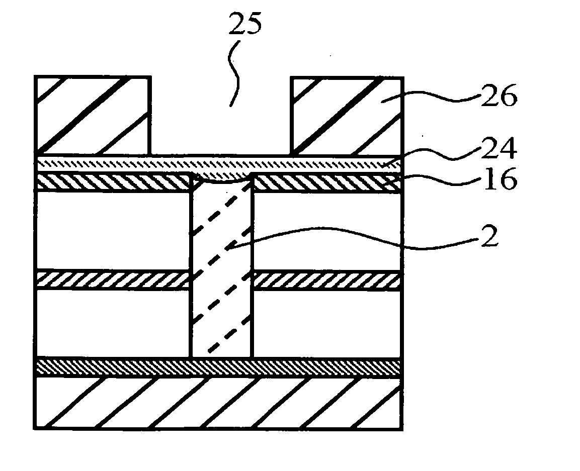
[0079] This shows the cross-sectional structure after the process of FIG. 5B, in which the dummy plug 2 was formed without conducting the etchback for the resin film 1. Here, same numeral is assigned to same element shown in FIGS. 2A through FIG. 5C. In addition, FIGS. 8A and 8B illustrate similar cross-sectional structures shown as comparative examples.

[0080] As shown in FIG. 6A, a via etch stop layer 12, which functions as an insulating barrier layer, was formed on a surface of an underlying interconnect 11. The via etch stop layer 12 was composed of a SiCN film. Here, an anti-corrosion material, which had been formed of a coating film of benzotriazole (BTA) in the previous process, for example, was formed on the surface of the underlying interconnect 11 composed of Cu. As a process bef...

example 2

[0088] Next, second example of the present invention will be described in reference to FIGS. 7A and 7B. FIG. 7A is also a cross-sectional view of a test element group (TEG) manufactured similarly as in the example shown in FIG. 6A. FIG. 7B is a scanning electron microscope (SEM) structure of a cross-section thereof. In case of example 2, the employed resin film 1 is different from that shown in FIG. 6A. The major difference therebetween is that no acidic agent is added to the resin film 1. Other configurations are same as that presented in FIG. 6A, as shown in FIG. 7A. Consequently, the following description focuses on the different points from the case of example 1. In this case, a resin film 1 containing a cellulose having a film thickness of 250 nm as a basic material was applied, and then, baked to be carbonized within nitrogen gas at 210 degree C.

[0089] Although a small hem-like bottom was generated in the bottom of the trench opening 25 formed in the second resist mask 26 in ...


PUM


Abstract

A method for manufacturing an electronic device, in which a via hole and a trench for an interconnect are integrally provided in an interlayer insulating film formed on a substrate, and the via hole and the trench for the interconnect are plugged with an electric conductor film is provided. The method includes: forming a via hole in the interlayer insulating film; forming a resin film, plugging the via hole, on the interlayer insulating film; forming a resist mask having an opening for an interconnect on the interlayer insulating film; and etching the interlayer insulating film through an etching mask of the resist mask to form a trench for the interconnect connected with the via hole. The resin film is being capable of trapping a basic substance.

Description

[0001] This application is based on Japanese patent application NO. 2004-317,719, the content of which is incorporated hereinto by reference. BACKGROUND [0002] 1. Technical Field [0003] The present invention relates to a method for manufacturing an electronic device. [0004] 2. Related Art [0005] In recent years, remarkably increasing processing speed of the semiconductor device leads to a problem of generating a transmission delay due to a decrease in a signal propagation rate, which is caused by an interconnect resistance in a multi-layer interconnect and a parasitic capacitance between the interconnects. Such problem tends to become more and more considerable, due to an increased interconnect resistance and an increased parasitic capacitance, which are caused in accordance with miniaturizations of a linewidth and an interconnect interval created by an increased integration of the semiconductor device. Consequently, in order to prevent a signal delay caused on the basis of enhancem...

Claims


Application Information

Patent Timeline
IPC IPC(8): H01L21/4763
CPCH01L21/76808
Inventor SODA, EIICHIYABE, SACHIKO
Owner RENESAS ELECTRONICS CORP
Why Eureka
Try Eureka