

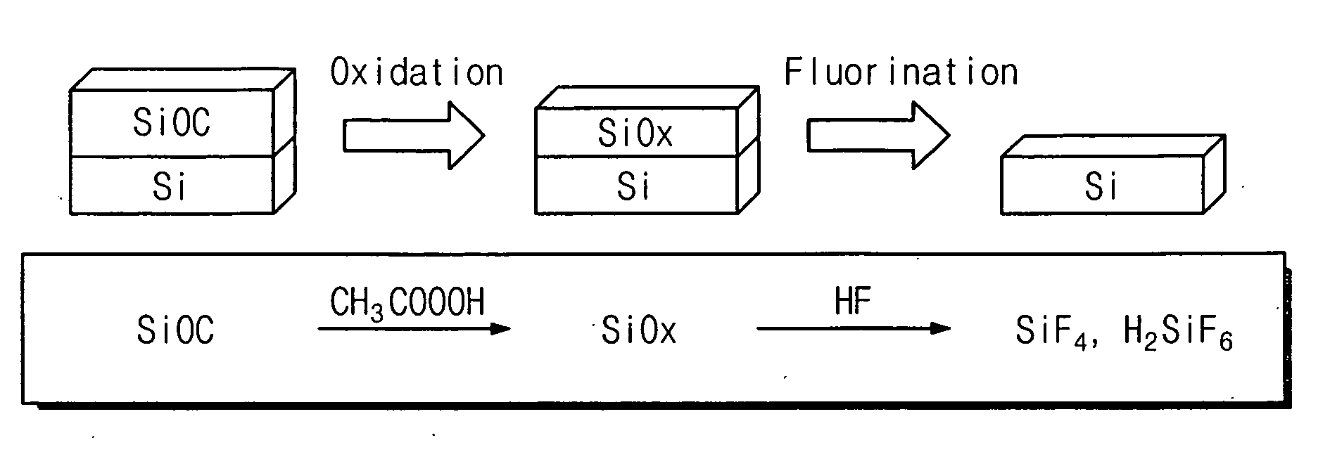
Etching solution and method for removing low-k dielectric layer
a dielectric layer and etching solution technology, applied in the preparation of detergent mixture compositions, detergent compositions, chemistry apparatus and processes, etc., can solve the problems of increasing the power consumption of the element, reducing the speed of the semiconductor element, and increasing the level of cross-talk, so as to achieve the effect of easy preparation, easy to obtain, and low cost of a reagen
- Summary
- Abstract
- Description
- Claims
- Application Information
AI Technical Summary
Benefits of technology
Problems solved by technology
Method used
Image

Examples
experiment 1
[0045] (Experiment 1)
[0046] Experiment 1 was performed in order to demonstrate the influence of the surfactant on etching. In the present experiment 1, the etching ratios of two etching solutions in accordance with this invention were compared for their effectiveness in etching the low-k dielectric layer. In a first case, the low-k dielectric layer etching solution (first etching solution) consisted essentially of 90 volume % of CH3COOOH and 10 volume % of HF each of which was suitably diluted. In a second case, the low-k dielectric layer etching solution (second etching solution) additionally included a surfactant by adding about 0.6 volume % of nonionic surfactant to the first etching solution. The etching ratios were measured respectively at about 25° C. FIG. 5 graphically illustrates the results of experiment 1. Referring to FIG. 5, it can be seen that the etching ratio of the first etching solution (that did not include the surfactant) was about 280 Å / min., while the etching ra...
experiment 2
[0047] (Experiment 2)
[0048] Experiment 2 was performed in order to compare the etching ability of different etching solutions in accordance with this invention based on the kind of oxidant included in the etching solution. In experiment 2, the etching ratios of an etching solution (third etching solution) including H2O2 as oxidant and of an etching solution (fourth etching solution) including CH3COOOH (PAA) as oxidant were measured and compared. Similar to the conditions used for experiment 1, etching was performed at about 25° C. The third etching solution consisted essentially of 90 volume % of H2O2, 10 volume % of HF, each of which was suitable diluted, and 0.6 volume % of surfactant. The fourth etching solution consisted essentially of 90 volume % of PAA, 10 volume % of HF, each of which was suitably diluted, and 0.6 volume % of surfactant, similar to the second etching solution (experiment 1 above). The results of experiment 2 are illustrated in FIG. 6.
[0049] Referring to FIG....
experiment 3
[0050] (Experiment 3)
[0051] Experiment 3 was performed in order to demonstrate the influence of the amount of the oxide etchant included in the etching solution, in particular the amount of HF, on the etching results. An etching solution (fifth etching solution) that included 10 volume % of HF was compared with an etching solution (sixth etching solution) that included 20 volume % of HF. The fifth etching solution consisted essentially of 90 volume % of CH3COOOH, 10 volume % of HF, each of which was suitably diluted, and 0.6 volume % of surfactant, similar to the second etching solution (experiment 1 above). The sixth etching solution consisted essentially of 80 volume % of CH3COOOH, 20 volume % of HF, each of which was suitably diluted, and 0.6 volume % of surfactant. Experiment 3 was performed both at about 25° C. and at about 65° C. The results of experiment 3 are illustrated in FIG. 78. In FIG. 78, the symbol ♦ (a small hollow square) is used to represent the etching ratio of th...
PUM
| Property | Measurement | Unit |
|---|---|---|
| Percent by volume | aaaaa | aaaaa |
| Percent by volume | aaaaa | aaaaa |
| Percent by volume | aaaaa | aaaaa |
Abstract
Description
Claims
Application Information