
Semiconductor device, IC card, IC tag, RFID, transponder, paper money, valuable securities, passport, electronic device, bag, and clothes

a technology of semiconductor devices and micro-conductor chips, applied in thermoelectric devices, instruments, nanoinformatics, etc., can solve the problems of difficult to achieve a good nonvolatile memory, inability to perform high-temperature treatment over 600° c., and small amount of data stored in a barcod

Inactive Publication Date: 2006-05-11
SEMICON ENERGY LAB CO LTD
View PDF12 Cites 48 Cited by
  • Summary
  • Abstract
  • Description
  • Claims
  • Application Information

AI Technical Summary

Benefits of technology

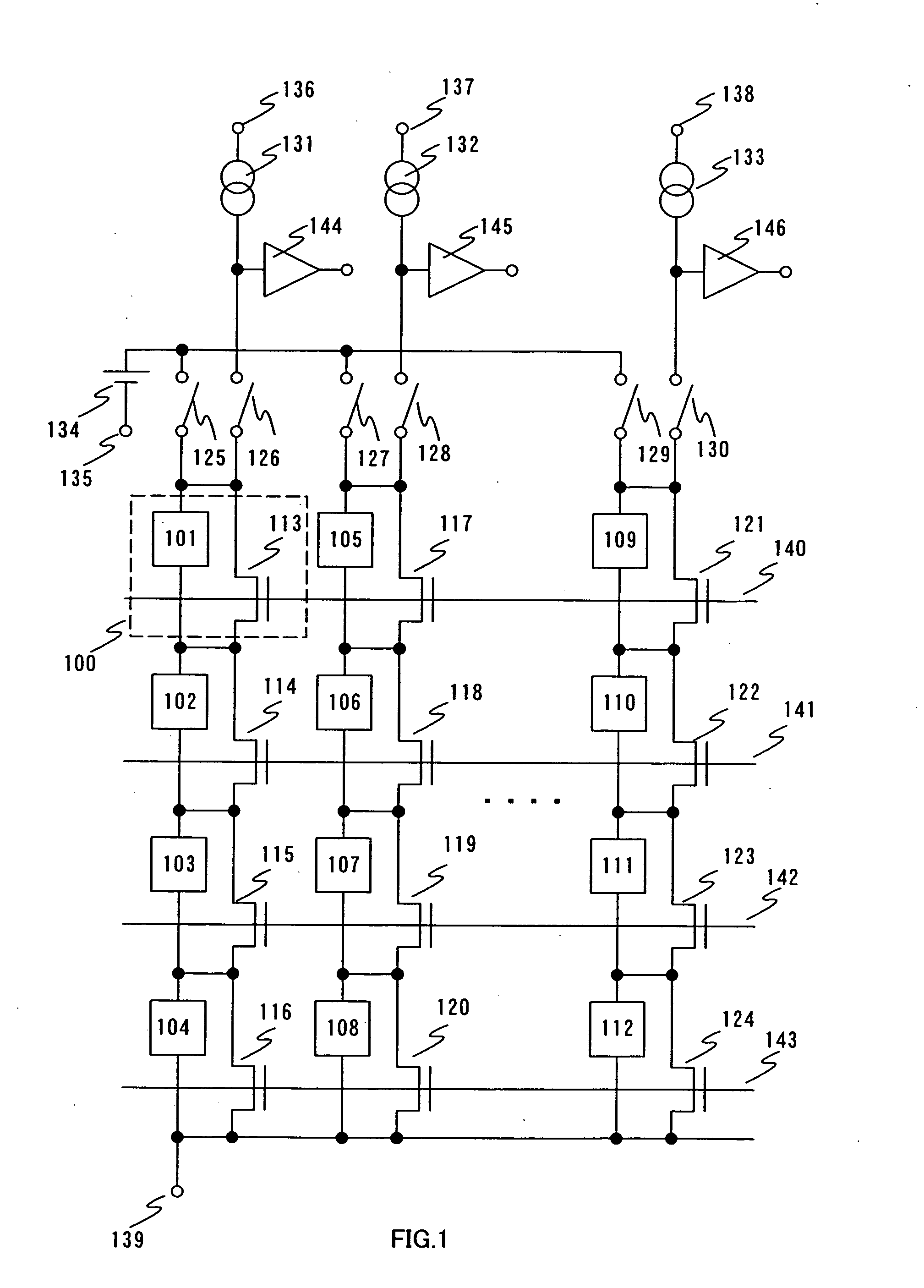
The invention provides a semiconductor device that uses a nonvolatile memory without using a high-performance gate insulating film that needs low-temperature manufacturing. The device includes a plurality of memory cells connected in parallel and in series, with each cell having an organic element and a transistor. The organic element can vary its conductivity or electric resistance when exposed to light, voltage, or current. The device can detect the signal of each memory cell column using a means at one end of each column. The invention also includes an RFID with the semiconductor device and various circuits for data processing and control. The invention can be used in various applications such as IC cards, IC tags, RFIDs, and electronic devices.

Problems solved by technology

However, data reading or the like using a barcode is disadvantageous in that a barcode reader is required to contact the barcode and the amount of data stored in a barcode is not very large.
However, when the transistor is formed over an insulating substrate such as glass, high-temperature treatment over 600° C. cannot be performed.
Accordingly, the quality of the gate insulating film can be improved only to a limited degree, which makes it difficult to achieve a good nonvolatile memory.

Method used


Image

  • Semiconductor device, IC card, IC tag, RFID, transponder, paper money, valuable securities, passport, electronic device, bag, and clothes
  • Semiconductor device, IC card, IC tag, RFID, transponder, paper money, valuable securities, passport, electronic device, bag, and clothes
  • Semiconductor device, IC card, IC tag, RFID, transponder, paper money, valuable securities, passport, electronic device, bag, and clothes

Examples


embodiment 1

[0085] A cross-sectional structure of a semiconductor device of the invention is described (see FIG. 22). Shown herein is a cross-sectional structure of a transistor 240 and an organic element 241 included in a memory array 222, and a CMOS circuit 248 included in a switch, a sense amplifier, or the like (denoted by 225 in FIG. 22). As for a substrate 230 of the invention, a quartz substrate, a silicon substrate, a metal substrate, a stainless substrate, or the like is used as well as a glass substrate or a flexible substrate. A flexible substrate means a substrate capable of being flexibly bent, such as a plastic substrate formed using polycarbonate, polyarilate, polyether sulfone, or the like.

[0086] The organic element 241 corresponds to a stack of a first conductive layer 243, an organic compound layer 244, and a second conductive layer 245, and an insulating layer 249 is provided between the adjacent organic elements 241. FIG. 22 shows an example of a NOR memory circuit, and the...

embodiment 2

[0093] When data writing is performed by means of light, one or both of the first conductive layer 243 and the second conductive layer 245 transmit light. The conductive layer which transmits light is formed using a light-transmissive conductive material such as indium tin oxide (ITO) or formed with a thickness to transmit light even if the material is not a light-transmissive conductive material.

[0094] For the organic compound layer 244, an organic compound material having conductivity can be used, and for example, substances which have high hole-transporting property can be used; namely, an aromatic amine compound (that is, a compound containing a bond of benzene ring—nitrogen) such as 4,4′-bis[N-(1-naphthyl)-N-phenyl-amino]-biphenyl (abbreviated to α-NPD), 4,4′-bis[N-(3-methylphenyl)-N-phenyl-amino]-biphenyl (abbreviated to TPD), 4,4′,4″-tris(N,N-diphenyl-amino)-triphenylamine (abbreviated to TDATA), 4,4′,4″-tris[N-(3-methylphenyl)-N-phenyl-amino]-triphenylamine (abbreviated to ...

embodiment 3

[0099] Next, data writing by means of an optical function is described. In this case, the organic compound layer 244 is irradiated with laser light from a light-transmissive conductive layer side (the second conductive layer 245 herein). Here, the organic compound layer 244 at a desired portion is selectively irradiated with the laser light to destroy the organic compound layer 244. The destroyed organic compound layer 244 is insulated, and thus the electric resistance thereof becomes considerably large compared to that of the other portion. Data writing is performed by utilizing the phenomenon that the electric resistance between two conductive films provided with the organic compound layer 244 interposed therebetween varies by the laser irradiation in this manner. For example, provided that a non-laser-irradiated organic compound layer has data of ‘0’, in order to write data of ‘1’, the electric resistance is increased by selectively irradiating the organic compound layer at a des...


PUM


Abstract

It is an object to provide a semiconductor device the data writing of which can be performed except in manufacturing and the counterfeiting of which by rewriting can be prevented. Furthermore, it is another object of the invention to provide a semiconductor device constituted by an organic memory having a simple structure at low cost. A memory cell is constituted by connecting a transistor in parallel or series to an organic element having an organic compound layer, and each memory cell is connected in series or parallel to constitute a NAND memory or a NOR memory. The organic element can change its electrical property irreversibly by application of a current or a voltage, irradiation of light, or the like.

Description

BACKGROUND OF THE INVENTION [0001] 1. Field of the Invention [0002] The present invention relates to a semiconductor device having an organic element. In particular, the invention relates to a semiconductor device having a memory circuit using an organic element. [0003] 2. Description of the Related Art [0004] In accordance with the development of computer technology and improvement of image recognition technology, data recognition using a medium such as a barcode has been widely used, which is used, for example, for data recognition of merchandise. A further larger amount of data recognition is expected to be processed in the future. However, data reading or the like using a barcode is disadvantageous in that a barcode reader is required to contact the barcode and the amount of data stored in a barcode is not very large. Therefore, data recognition without contact and increase of the memory capacity of a medium have been demanded. [0005] In response to such demand, an ID chip using...

Claims


Application Information

Patent Timeline
Patent Type & Authority Applications(United States)
IPC IPC(8): H01L29/08H01L29/04
CPCB82Y10/00G11C13/0014G11C13/0059H01L27/285H01L28/10H10K19/10H10K19/202
Inventor KOYAMA, JUNABE, HIROKOYUKAWA, MIKIOIWAKI, YUJIYAMAZAKI, SHUNPEI
Owner SEMICON ENERGY LAB CO LTD
Learn More