Method of reducing the average process bias during production of a reticle

a technology of lithographic mask and process, applied in the field of lithographic mask production, can solve the problems of process bias, loss of resolution, process window for this feature size which would enable a manufacturing process, etc., and achieve the effect of improving the etch resistance of the pattern developed photoresist and the size of the developed photoresist mask features

Inactive Publication Date: 2006-05-18
APPLIED MATERIALS INC
View PDF15 Cites 5 Cited by
  • Summary
  • Abstract
  • Description
  • Claims
  • Application Information

AI Technical Summary

Benefits of technology

[0019] The improvement in average process bias is achieved by treating the developed photoresist pattern on the reticle substrate prior to dry etching of the pattern into the pattern transfer layer of the reticle. The developed photoresist pattern is treated with a silicon-containing reagent to enlarge the developed photoresist pattern on its exterior surface. The effect of the treatment is greater at pattern locations where there is increased surface area to volume, such as at the corners at the ends of lines. This helps compensate for the more rapid development and rounding of such areas during development of the photoresist pattern.
[0021] The silicon-containing reagents include hexamethydisilazane (HMDS); trimethylsilyldiethylamine (TMSDEA); N,N-dimethylaminotrimethylsilane (TMSDMA); 1,1,3,3-tetramethyldisilazane (TMDS), dimethylsilyldiethylamine (DMSDEA); dimethylsilyldimethylamine (DMSDMA); hexamethylcyclotrisilazane (HMCTS); bis(N,N-dimethylamino)dimethylsilane (BDADS); and bis(N,N-dimethylamino)methylsilane (BDAMS), for example and not by way of limitation. The latter three materials are polyfunctional or cyclic materials, which tend to provide a larger volume increase in the developed photoresist exterior surfaces for a given amount of silicon-containing reagent consumed during the treatment. The polyfunctional materials, such as a nitrogen substituted silanes, for example, enable crosslinking at the surface of the silylated photoresist, providing improved thermal stability of the photoresist and increased etch resistance during pattern transfer to the underlying radiation-blocking mask material (such as the metal-containing layers described herein, by way of example.)
[0023] In addition to increasing the size of the developed photoresist mask features (and thereby the size of the reticle features generated from the photoresist mask), the method of the invention typically improves the etch resistance of the pattern developed photoresist during transfer of the pattern from the photoresist to the pattern transfer layer (typically comprising chrome) of the reticle. One skilled in the art will recognize that the method of the present invention can be used in combination with any direct write imaging tooling used to produce reticles, including electron beam tooling as well as continuous write laser tooling.

Problems solved by technology

As disclosed in the '394 patent, there are a number of problems encountered in trying to produce a photomask / reticle when the photomask pattern exhibits critical dimensions of less than 0.25 Φm (250 nm).
One of the more important problem areas is the process bias which occurs, in part, as a result of the wet development of the photoresist which is used to pattern the reticle.
As the developed pattern dimensions have become smaller, portions of the pattern are dissolved away during the wet development, leading to a loss in resolution in the etched thin metal-containing layer of the reticle which is patterned to produce a “hard copy” of the individual device structure pattern to be recreated on the semiconductor substrate masking layer.
Currently the smallest feature which can be written using an optical continuous wave laser writing tool of the kind described herein is about 175 nm; however, at present there is no process window for this feature size which would enable a manufacturing process.
Although it is possible to write a 180 nm latent image in the photoresist, for example a square which is 180 nm on a side, this assist feature is sufficiently small that it typically cannot be properly imaged (printed) using optical imaging techniques.

Method used


Image

  • Method of reducing the average process bias during production of a reticle
  • Method of reducing the average process bias during production of a reticle
  • Method of reducing the average process bias during production of a reticle

Examples


example two

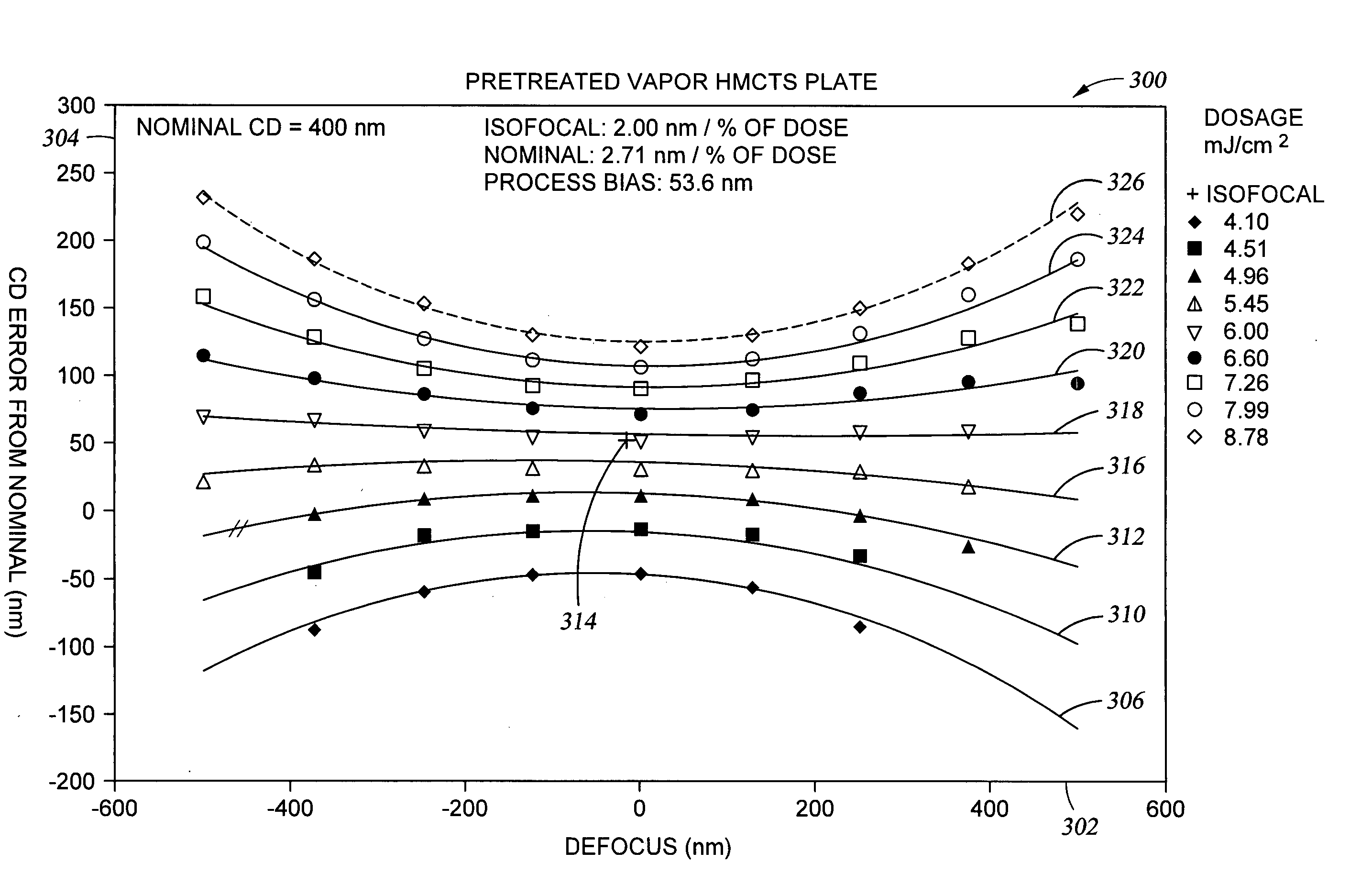
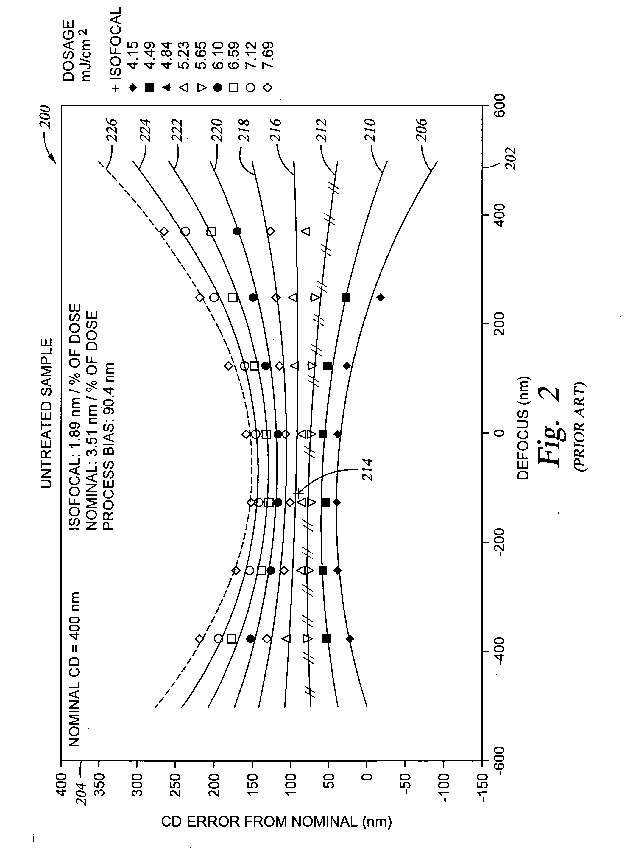
[0048] The reticle substrate which was used to prepare test specimens for the example embodiments of the invention was the same as that used to prepare the test specimens for the comparative Example One, with the exception that the developed, patterned photoresist was treated subsequent to the spin dry cycle of the development process. The photoresist was treated with a silicon-containing reagent to add volume to the developed pattern feature size.

[0049] There are two different methods which may be used for treatment with a silicon-containing agent, a vapor phase reaction and a wet phase reaction. The data shown in FIG. 3 was for a vapor phase treatment with a silicon-containing agent. In the vapor phase reaction, the test specimen reticle plate was placed in a Y.E.S.—1224 vacuum oven, available from Yield Engineering Systems of Santa Clara, Calif. This large vacuum oven provides temperature uniformity (±2 EC). The system pumps down in the range of about 1 Torr, and purges up to ne...


PUM

PropertyMeasurementUnit
wavelengthsaaaaaaaaaa
feature sizeaaaaaaaaaa

Abstract

We are able to reduce the average process bias in a patterned reticle by treating the developed, patterned photoresist which is used to transfer a pattern to the reticle with a silicon-containing reagent prior to the pattern transfer. The process bias is a measure of the difference between a nominal feature critical dimension (CD) produced in a patterned reticle and the nominal isofocal CD for the feature. Improvement of the average process bias is directly related to an improved resolution in the mask features. The reduction in average process bias achievable using the method of the invention typically ranges from about 30% to about 70%. This reduction in average process bias enables the printing of smaller features.

Description

CROSS REFERENCE TO RELATED APPLICATIONS [0001] This application is related to U.S. application Ser. No. 10 / 261,972, filed Sep. 30, 2002, titled: “Method of Producing A Patterned Photoresist Used To Prepare High Performance Photomasks”, which is currently pending. This application is also related to U.S. Pat. No. 6,605,394 issued Aug. 12, 2003, titled: “Organic Bottom Antireflective Coating For High Performance Mask Making”. This application is also related to U.S. Pat. No. 6,703,169, issued Mar. 9, 2004, titled: “Method Of Preparing Optically Imaged High Performance Photomasks”.BACKGROUND OF THE INVENTION [0002] 1. Field of the Invention [0003] In general, the present invention relates to a method of producing a lithographic mask (reticle) for use in the semiconductor industry. In particular, the invention pertains to a method of producing a patterned photoresist used in preparation of the reticle. The optical imaging of the photoresist makes use of a deep ultraviolet (DUV) radiatio...

Claims


Application Information

Patent Timeline
Patent Type & Authority Applications(United States)
IPC IPC(8): G03C1/494G03C1/492G03C5/00G03C1/76G03F1/00
CPCG03F7/405Y10S430/143
Inventor MONTGOMERY, MELVIN WARRENBUXBAUM, ALEXANDER
Owner APPLIED MATERIALS INC
Why Eureka
Try Eureka