CMOS-MEMS process

a technology of metal oxides and mems, applied in the field of complementary metal oxidesemiconductor (cmos) microelectromechanical system (mems) process, can solve the problems of easy deterioration of circuit performance, inability to propose evidence, damage to transistors, etc., to avoid the drawbacks of device performance deterioration and structure damage, increase process flexibility, and reduce cost

Active Publication Date: 2006-05-18
NAT APPLIED RES LAB
View PDF2 Cites 17 Cited by
  • Summary
  • Abstract
  • Description
  • Claims
  • Application Information

AI Technical Summary

Benefits of technology

[0007] From an aspect of the present invention, PR is used to replace the metal layer as a mask in post etching process, avoiding the drawbacks of device performance deterioration and structure damages resulted from the metal layer mask in conventional p...

Problems solved by technology

However, there are many drawbacks in the previous COMS-MEMS process, for examples, input/output (I/O) pads including electrostatic discharge (ESD) circuits are destroyed by ion bombardment, CMOS transistors are damaged if there is no metal layer above them, a floating metal layer induces more parasitics and is not allowed especially in RF circuits, CMOS passivation layer is removed...

Method used


Image

  • CMOS-MEMS process
  • CMOS-MEMS process
  • CMOS-MEMS process

Examples


Embodiment Construction

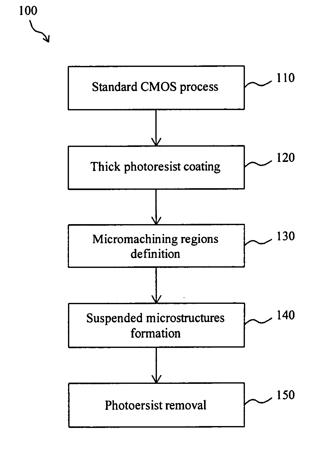
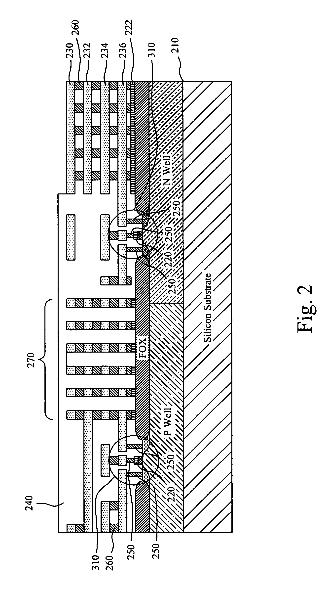
[0017]FIG. 1 shows a flowchart 100 of a CMOS-MEMS process according to the present invention. It starts with 0.35 μm double-poly quadruple-metal (2P4M) CMOS polycide process. After a standard CMOS process in step 110, as shown in FIG. 2, electronic circuits 310 and microstructures 270 are formed on a substrate 210. The microstructures 270 of MEMS components consist of polysilicon 222, metal layers 230, 232, 234 and 236, and dielectrics 240. The electronic circuits 310 include active devices and their corresponding contacts 250, vias 260 and interconnections 234 and 236. The first polysilicon layer 220 for forming the electronic circuits 310 can not interconnect to the second polysilicon layer 222. The contact holes between the metal layer 236 and the sources, drains and gates of the active devices, and the via holes between the multiple metallization layers 230-236, are filled with tungsten plugs to form the contacts 250 and vias 260. The multiple metallization layers 230-236 are ma...


PUM


Abstract

A fully CMOS compatible MEMS multi-project wafer process comprises coating a layer of thick photoresist on a wafer surface, patterning the photoresist to define a micromachining region, and performing a micromachining in the micromachining region to form suspended microstructures.

Description

REFERENCE TO RELATED APPLICATIONS [0001] This Application is based upon Provisional Application Ser. No. 60 / 626,923, filed 12 Nov. 2004.FIELD OF THE INVENTION [0002] The present invention is generally related to a complementary metal-oxide-semiconductor (CMOS) microelectromechanical system (MEMS) process and, more particularly, to a fully CMOS compatible MEMS multi-project wafer process. BACKGROUND OF THE INVENTION [0003] Surface and bulk micromachining technologies combined with the existing integrated circuit (IC) technologies have more and more potential to serve as a system-on-chip (SoC) design platform. New ideas can be rapidly implemented through the mature foundry service without worrying about the process complexity. High-aspect-rate CMOS-MEMS process was first reported by G. K. Fedder et al., Proc. MEMS '96, pp. 13-18, 1996. Top metal layer in this technology acts as a hard mask while performing post etching process. Up to now, it has been applied to make mechanical filter,...

Claims


Application Information

Patent Timeline
IPC IPC(8): H01L21/30
CPCB81C1/00246B81C2203/0735H01L21/764H01L27/0617H01L27/08H01L28/10
Inventor XIAO, FU-YUANJUANG, YING-ZONGCHIU, CHIN-FONG
Owner NAT APPLIED RES LAB
Why Eureka
Try Eureka