Process for fabricating semiconductor device

a technology of semiconductor devices and fabrication processes, applied in semiconductor devices, electrical devices, transistors, etc., can solve the problems of thermal influence on the substrate, low productivity, and inferior physical properties of crystalline silicon semiconductors, so as to prevent heat damage on the substrate, improve crystal character, and improve the effect of crystal character

Inactive Publication Date: 2006-06-01
SEMICON ENERGY LAB CO LTD
View PDF38 Cites 17 Cited by
  • Summary
  • Abstract
  • Description
  • Claims
  • Application Information

AI Technical Summary

Benefits of technology

[0022] If these metal elements are included in the silicon film, it is also possible to crystallize the silicon film at a lower temperature in the process of RTA later. These metal elements also have an effect of promoting elimination (ejection) of hydrogen from the amorphous silicon film during thermal annealing. If silicon ions have been implanted to the silicon film as above mentioned before thermal annealing process, crystallization growth during thermal annealing can be suppressed, which is preferable, even if these metal elements are added.
[0024] As a light to be utilized for RTA in the second step above mentioned, it is preferable if wavelength of the light to be utilized is absorbed in the silicon film but is not substantially absorbed to the glass substrate. That is, it is preferable if the center wavelength lies in the near infrared radiation or visible light. For example, a light with wavelength of 4 μm to 0.6 μm is desirable (e.g. infrared light having a peak at wavelength 1.3 μm). By irradiating intense light like this for relatively a short time like 10 to 1000 seconds, the silicon film can be heated and crystal character can be improved. It is desirable if the silicon film is heated at 800 to 1300° C.
[0025] If the silicon film is suddenly heated from a room temperature to a high temperature like this, or on the contrary if the silicon film is suddenly cooled from a high temperature like this to a room temperature, effect of stress and the like to be taken on the silicon film is big. Therefore preheat process to heat the film at a lower temperature than this high temperature, or post heat process to heat the silicon film at a temperature between this high temperature and the room temperature for a while in the course of descending temperature from the high temperature condition can be provided. To prevent heat damage on the substrate, it is preferable if temperature of the preheat process and the postheat process is lower than the strain point of the glass substrate by 50 to 200° C.
[0026] By thermal annealing in the first process, a nucleus of crystal growth is at least generated, and a low crystallized silicon film (crystallized area is 1 to 50%, preferably 1 to 10% (the rest is amorphous condition)) can be obtained even if the crystallization is suppressed. However, it is not preferred that a semiconductor device is formed by directly using the crystalline silicon film obtained by the first step. This is because there are left a lot of amorphous components mainly in the grain boundary and characteristic of the silicon film is not preferable in bulk and surface thereof. In the present invention, this silicon film is converted to a silicon film with good crystal character by RTA of the second process. By RTA, the silicon film is heated, and crystallinity of the crystallized silicon film is improved and the film is densified simultaneously. In this time, in case that the silicon film has a low crystallinity degree, crystallization can be expanded from the crystal nuclei formed by the first step to the surrounding amorphous region. In this case, since the crystallization proceeds relatively long distance, the effect of decreasing grain boundaries is obtained. By improving the crystallinity in this manner, the high quality silicon film with 90% or more thereof in area being crystallized can be obtained, which can be utilized for a thin film transistor (TFT).
[0027] However, in such RTA, temperature partially changes rapidly. Thus because of difference in thermal expansion coefficient between the silicon film and the substrate, and difference of temperature between the surface of the silicon film and the interface of the substrate and the silicon film, the silicon film is often peeled off. This is particularly notable in the case that the area of the film is so big that it covers the whole surface of the substrate. Therefore, peeling and the like of the film can be prevented by dividing the film in sufficiently small areas, and by making distances between the divided films sufficiently wide so that unnecessary heat would not be absorbed by the substrata. In this way, because the whole surface of the substrate will not be heated through the silicon film, thermal shrinkage of the substrate is suppressed mostly.

Problems solved by technology

The physical properties thereof, such as electric conductivity, however, are still inferior to those of a crystalline silicon semiconductor.
However, such a high temperature heating has a problem of thermally influencing the substrate.
Furthermore, since the heating time required for crystallization was several tens hours or longer, productivity was low.
However, since the film formed by plasma CVD and low pressure CVD contains a lot of hydrogen combined with silicon, the decomposition reaction of hydrogen is mainly caused by RTA owing to the short time of RTA, that is, the crystallization does not sufficiently proceed.
Furthermore, there is a problem that hydrogen is ejected to the exterior of the film by the decomposition reaction of hydrogen to degrade the morphology of the film surface.

Method used


Image

  • Process for fabricating semiconductor device
  • Process for fabricating semiconductor device
  • Process for fabricating semiconductor device

Examples


example 1

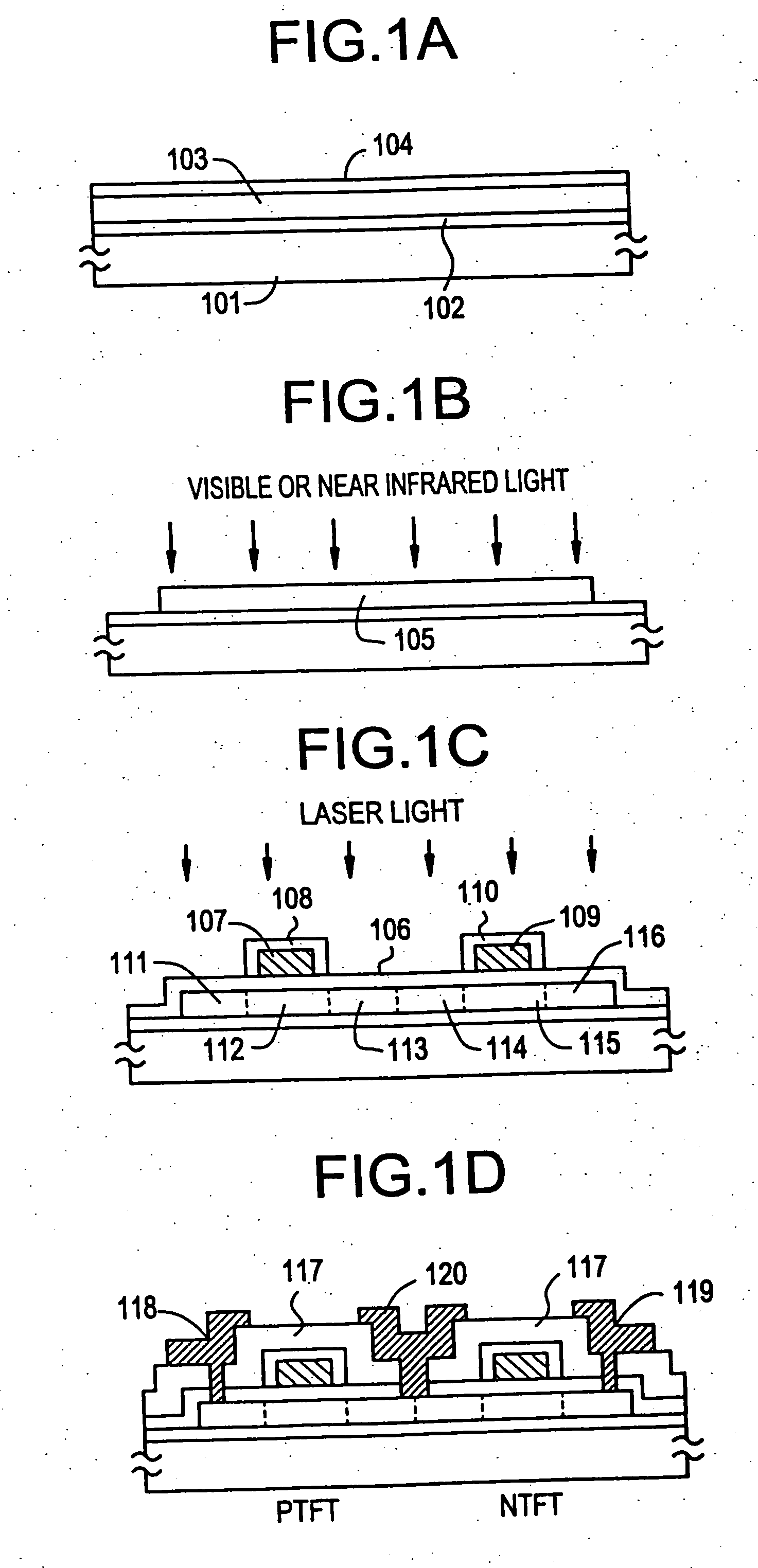
[0033] Referring to FIGS. 1(A) to 1(D), the present example relates to a process for fabricating a circuit comprising a p-channel TFT (hereinafter referred to simply as a “PTFT”) and an n-channel TFT (hereinafter referred to simply as an “NTFT”) formed in a complementary arrangement using a crystalline silicon film formed on a glass substrate. The structure obtained in the present example is applicable to switching elements of pixel electrodes and to peripheral driver circuits of active liquid crystal display devices, as well as to image sensors and three-dimensional integrated circuits.

[0034] Referring to the cross section views in FIGS. 1(A) to 1(D), the fabrication process of the present example is described below. A 2,000 Å thick silicon oxide film was deposited as a base film 102 on the surface of a Coming 7059 glass substrate 101 by a sputtering process. Mask alignment in the later steps can be facilitated by annealing the substrate either before or after depositing the base ...

example 2

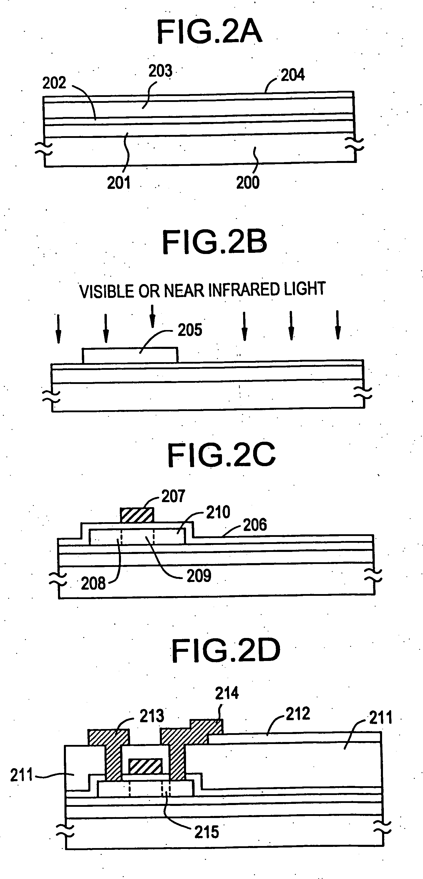
[0053] The present example relates to an active-matrix type liquid crystal display device having N-channel TFTs (NTFTs) each attached as a switching element to each of the pixels. The following description refers to a single pixel only, however, a practical active-matrix type liquid crystal device comprises a great number (generally several hundred thousands) of pixels all having the same structure simultaneously. Furthermore, the TFT not necessarily be an NTFT, and a PTFT can be employed as well. The TFT need not be provided to the pixel portion of the liquid crystal display, and it can be used in the peripheral circuits. Moreover, it can be used in image sensors and in other devices. In short, the application is not limited as long as it is used as a thin film transistor.

[0054] Referring to the step sequential structures shown in FIGS. 2(A) to 2(D), the process for fabricating the structure according to an embodiment of the present invention is described below. A 2,000 Å thick fi...

example 3

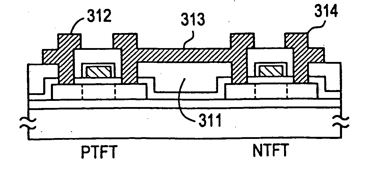
[0061] Referring to FIGS. 3(A) to 3(E), a process for fabricating a TFT circuit according to an embodiment of the present invention is described below. A substrate of a glass having a strain point in the range of from 550 to 650° C., such as an AN2 glass substrate having a strain point of 616° C., was used. To prevent shrinking from occurring, the substrate was subjected previously to pre-annealing at 670° C. for a duration of 4 hours and to cooling to 450° C. at a rate of 0.1° C. / min in a manner similar to that in Example 1. A base film 302 was formed on the substrate 301, and an amorphous silicon film 303 having thickness from 300 to 800 Å and a 200 Å thick silicon oxide film 304 were deposited thereafter by plasma CVD. The resulting structure was heated for annealing at 620° C. for a duration of 30 minutes. After the thermal annealing, the substrate was rapidly cooled to 450° C. at a rate of from 2 to 200° C. / sec, preferably, at a rate of 10° C. / sec or higher. This treatment prev...


PUM

PropertyMeasurementUnit
with wavelengthaaaaaaaaaa
temperatureaaaaaaaaaa
surface temperatureaaaaaaaaaa

Abstract

A process for fabricating a semiconductor device comprising the step of, after patterning the silicon film crystallized to a low degree by thermally annealing an amorphous silicon film into an island by etching, irradiating an intense light of a visible light or a near infrared radiation to effect a short-period annealing (RTA) to the silicon film of low crystallinity. Thus, the crystallinity of the silicon film is improved and the silicon film is densified in a short-period.

Description

BACKGROUND OF THE INVENTION [0001] 1. Industrial Field of the Invention [0002] The present invention relates to a process for fabricating an insulated gate-structured semiconductor device such as a thin film transistor (TFT) or a thin film diode (TFD), comprising a non-single crystal silicon film formed on an insulating substrate such as a glass substrate or on an insulating film formed on various type of substrate. The present invention also relates to a process for fabricating a thin film integrated circuit (IC) to which TFT or TFD is applied, and more particularly, to a thin film integrated circuit (IC) for an active-matrix type liquid crystal displaying unit. [0003] 2. Prior Art [0004] Semiconductor devices developed heretofore comprising TFTs on an insulating substrate (such as a glass substrate) include an active matrix-addressed liquid crystal display device whose pixels are driven by TFTs, an image sensor, or a three-dimensional integrated circuit. [0005] The TFTs utilized i...

Claims


Application Information

Patent Timeline
Patent Type & Authority Applications(United States)
IPC IPC(8): H01L29/04H01L21/336H01L21/20H01L21/77H01L21/84H01L29/786
CPCH01L21/02422H01L21/02488H01L21/02532H01L21/02667H01L21/02672H01L27/1285H01L29/66757H01L29/78624H01L27/1277H01L27/1281H01L21/02686H01L21/18
Inventor TAKEMURA, YASUHIKO
Owner SEMICON ENERGY LAB CO LTD
Why Eureka
Try Eureka