Single-pass growth of multilayer patterned electronic and photonic devices using a scanning localized evaporation methodology (SLEM)

Inactive Publication Date: 2006-06-08
OPTOELECTRONICS SYST CONSULTING
View PDF3 Cites 8 Cited by
  • Summary
  • Abstract
  • Description
  • Claims
  • Application Information

AI Technical Summary

Benefits of technology

[0012] This invention describes an apparatus for the close proximity deposition of thin films with high feature definition, higher deposition rates, and significantly improved material economy. The device loads the surface of fixed heating elements, made of thin films (20 A-20000 A), with evaporable material. The loaded thin film heating element is transported to the substrate site for the re-evaporation. The re-evaporation takes place through a mask onto a substrate maintained at the desired temperature. The mask, which comprises a pattern, dictated by the structural requirements of the device under fabrication, may be heated to prevent clogging. The translation of the substrate past the evaporation site replicates the pattern on its entire surface. The above cycle is herein termed as Scanning Localized Evaporation Methodology (SLEM). A multiplicity of evaporation sites through multiple SLEM fixtures is provided that can operate in parallel. Multilayered structures of evaporable materials with high in-plane spatial resolution can be deposited using this apparatus.
[0019] (5) A means of heating the shadow mask to prevent undesirable clogging of the fine features.
[0021] OLED-based full color flat panel displays (FPDs), thin film electronic devices and photonic band gap structures, which conventionally employ multi-batch fabrication processes, can now be realized in one continual in-line vacuum system equipped with multi-segment SLEM rotors. The ability to tightly control both the patterning-resolution and layer thicknesses, particularly in multilevel structures, results in increased throughput while maintaining superior device performance.

Problems solved by technology

[9] This process is limited to relatively large feature sizes.
[11] These techniques, however, have a number of limitations, such as cost associated with background patterning and multi-step batch processing.

Method used


Image

  • Single-pass growth of multilayer patterned electronic and photonic devices using a scanning localized evaporation methodology (SLEM)
  • Single-pass growth of multilayer patterned electronic and photonic devices using a scanning localized evaporation methodology (SLEM)
  • Single-pass growth of multilayer patterned electronic and photonic devices using a scanning localized evaporation methodology (SLEM)

Examples


Embodiment Construction

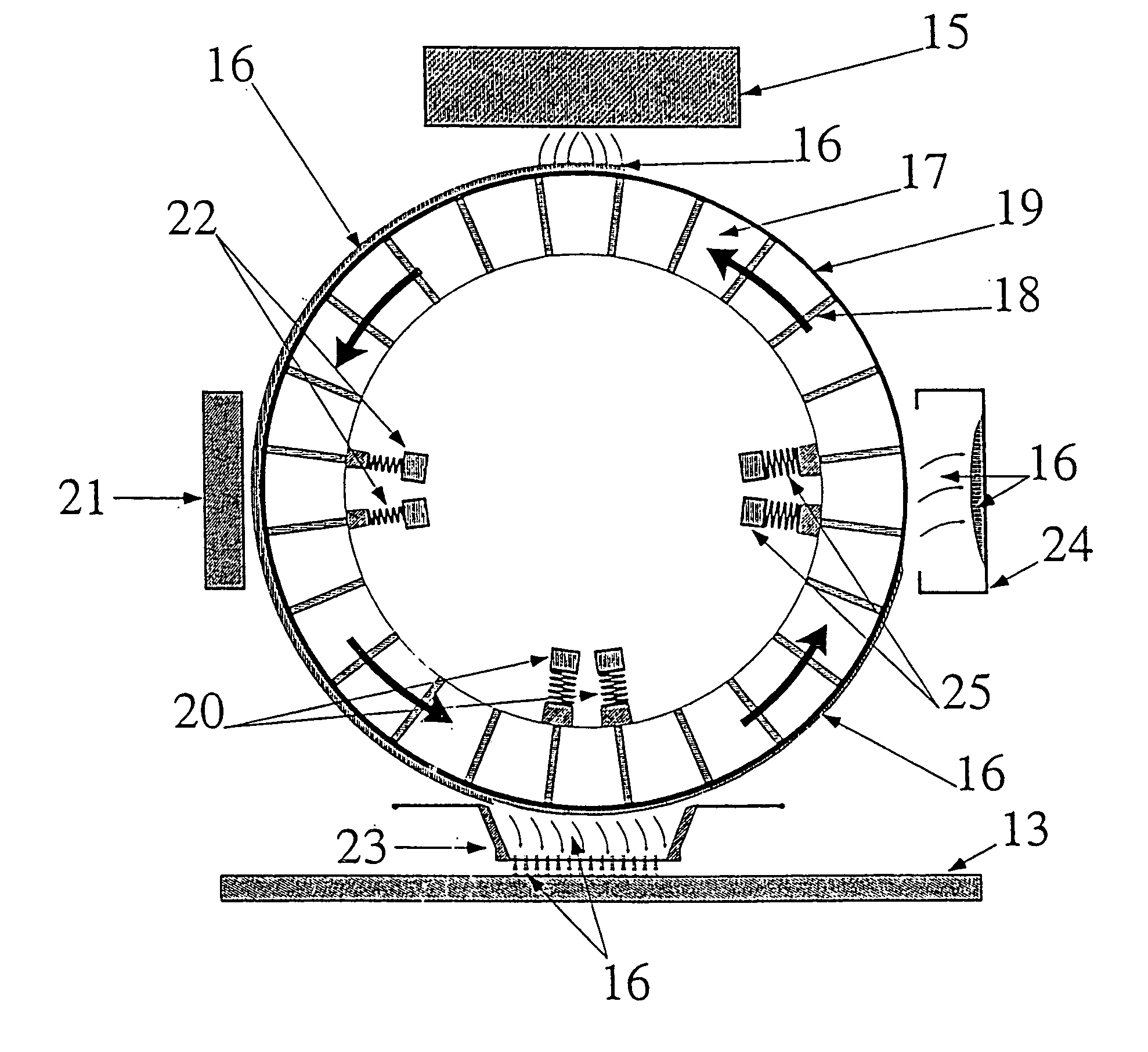
[0030]FIG. 3 depicts schematically the Scanning Localized Evaporation Methodology (SLEM) process for depositing thin films onto substrates, which are placed in close proximity to the deposition source. A thin film deposition cycle begins at the loading station, where evaporation of a sublimable material commences on to an array of heater elements. The heater elements are mounted on a first transport mechanism. The thickness of the deposited film on a selected heating element can be determined at the monitoring station, when this heating element is positioned opposite to the monitoring station by the first transport mechanism. The same transport mechanism also brings the loaded heating elements to the deposition site. Here, the thin film is re-evaporated and deposited through a mask onto a substrate. The substrate is mounted on a second transport mechanism that provides the means to move and index it relative to the mask. In the case where the substrate is larger than the mask patter...


PUM

PropertyMeasurementUnit
Temperatureaaaaaaaaaa
Circumferenceaaaaaaaaaa
Electrical resistivityaaaaaaaaaa

Abstract

The invention decribes an apparatus, Scanning Localized Evaporation Methodology (SLEM) for the close proximity deposition of thin films with high feature definition, high deposition rates, and significantly improved material economy. An array of fixed thin film heating elements, each capable of being individually energized, is mounted on a transport mechanism inside a vacuum chamber. The evaporable material is deposited on a heating element. The SLEM system loads the surface of heating elements, made of foils, with evaporable material. The loaded thin film heating element is transported to the substrate site for re-evaporation. The re-evaporation onto a substrate, which is maintained at the desired temperature, takes place through a mask. The mask, having patterned openings dictated by the structural requirements of the fabrication, may be heated to prevent clogging of the openings. The translation of the substrate past the evaporation site permits replication of the pattern over its entire surface. A multiplicity of fixed thin film heating element arrays is provided that can operate simultaneously or in sequence. Multi-layered structures of evaporable materials with high in-plane spatial pattern resolution can be deposited using this apparatus. In one version of the invention, the transport of the evaporant-loaded thin film heating elements is accomplished by the use of cylindrical rotors on whose circumference the heating elements are mounted.

Description

[0001] This application is a continuation-in-part of application Ser. No. 10 / 159,670, filed 0 / 03 / 2002, pending.BACKGROUND OF THE INVENTION [0002] 1. Field of the Invention [0003] This invention relates to the use of a scanning localized evaporation methodology for processing of multilayer, patterned electronic and photonic devices, such as transistors, sublimable organic light-emitting diodes (OLEDs), photonic band gap structures, and integrated circuits / systems. One example is the fabrication of displays using OLEDs for applications ranging from computer monitors to personal digital assistant (PDAs). [0004] 2. Description of the Related Art Introduction: [0005] A typical display screen comprises of a regular array of color pixels, each of which can be electrically selected to emit red, green and blue colored light, resulting in a desired shade and brightness. Each pixel is comprised of three devices, a red, a green, and a blue light-emitting element. Liquid crystal displays make u...

Claims


Application Information

Patent Timeline
IPC IPC(8): C23C16/00C23C14/04C23C14/24C23C14/26C23C14/56H01L51/56
CPCC23C14/042C23C14/246C23C14/26C23C14/568H01L51/56H10K71/40H10K71/164H10K71/00
Inventor PAPADIMITRAKOPOULOS, FOTIOSPHELY-BOBIN, THOMAS SAMUELGRANTHAM, DENIEL HARRISONJAIN, FAQUIR C.
Owner OPTOELECTRONICS SYST CONSULTING
Why Eureka
Try Eureka