Process to minimize and/or eliminate conductive material coating over the top surface of a patterned substrate

Inactive Publication Date: 2006-06-08
NOVELLUS SYSTEMS
View PDF55 Cites 18 Cited by
  • Summary
  • Abstract
  • Description
  • Claims
  • Application Information

AI Technical Summary

Benefits of technology

[0007] Removal of the large and non-uniform overburden of FIG. 2 from the patterned substrate surface and obtaining the structure in FIG. 3 with minimal dishing is difficult, time consuming, and expensive. We have recently disclosed methods and apparatus that can plate and polish or minimize accumulation of metal or metal alloy overburden and, therefore, yield a film 8 of conductive material such as Cu, with a uniform overburden 8a as depicted in FIG. 4. In this application, we disclose a method that minimizes the thickness of this overburden and even eliminates it through the use of electroche

Problems solved by technology

The example shown demonstrates an especially challenging case of metal filling and planarization procedures which are carried out with patterned substrate features having widely different sizes.
Removal of the large and non-uniform overburden of FIG. 2 from the patterned substrate surface and obtaining the structure in FIG. 3 with minimal dishing is difficult, time consuming, and expen

Method used


Image

  • Process to minimize and/or eliminate conductive material coating over the top surface of a patterned substrate
  • Process to minimize and/or eliminate conductive material coating over the top surface of a patterned substrate
  • Process to minimize and/or eliminate conductive material coating over the top surface of a patterned substrate

Examples


example 1

Standard Electrolyte Solution

[0041] A Cu-sulfate based Cu plating solution was prepared as follows:

[0042] 70 grams per liter of CuSO4+5H2O, 150 grams per liter of concentrated H2SO4, and 70 ppm per liter of Cl− ions were mixed in enough water to make 10 liters of solution. Twenty-five ml of Ultrafill S2001®, 1.0 ml of Ultrafill A2001® from Shipley were then added to obtain a standard good quality plating electrolyte.

[0043] This solution was used for Cu plating on a 200 mm diameter wafer surface. The wafer surface contained sub-micron size features as well as features in the 10-100 micron range. The pad was a fixed abrasive pad supplied by 3M® company. The diameter of the pad was 180 mm and the anode assembly was oscillated in the horizontal direction so that plating could be achieved on all areas on the larger wafer surface. During plating, the distance between the pad and the wafer surface was kept at around 0.1 cm. The plating current was 2 amperes and the plating solution flow...

example 2

Polishing and Planarization Using Standard Electrolyte Solution

[0044] The plating experiment of Example 1 was repeated, except this time, after an initial period of 30 seconds, the pad was pushed against the wafer surface at a pressure of 1 psi for plating as well as polishing and planarization. The resulting Cu deposit had a rough surface with deep scratches apparently caused by the abrasive pad. There were also Cu particles smeared all over the surface of the wafer. Very little amount of material removal was achieved because material removed from one region of the surface by the action of the abrasive pad was probably deposited back onto the surface at another region in the form of smeared particles, which were welded or bonded to the substrate surface. The substrate defect level was extremely high and feature filling was poor.

example 3

Modified Electrolyte Solution

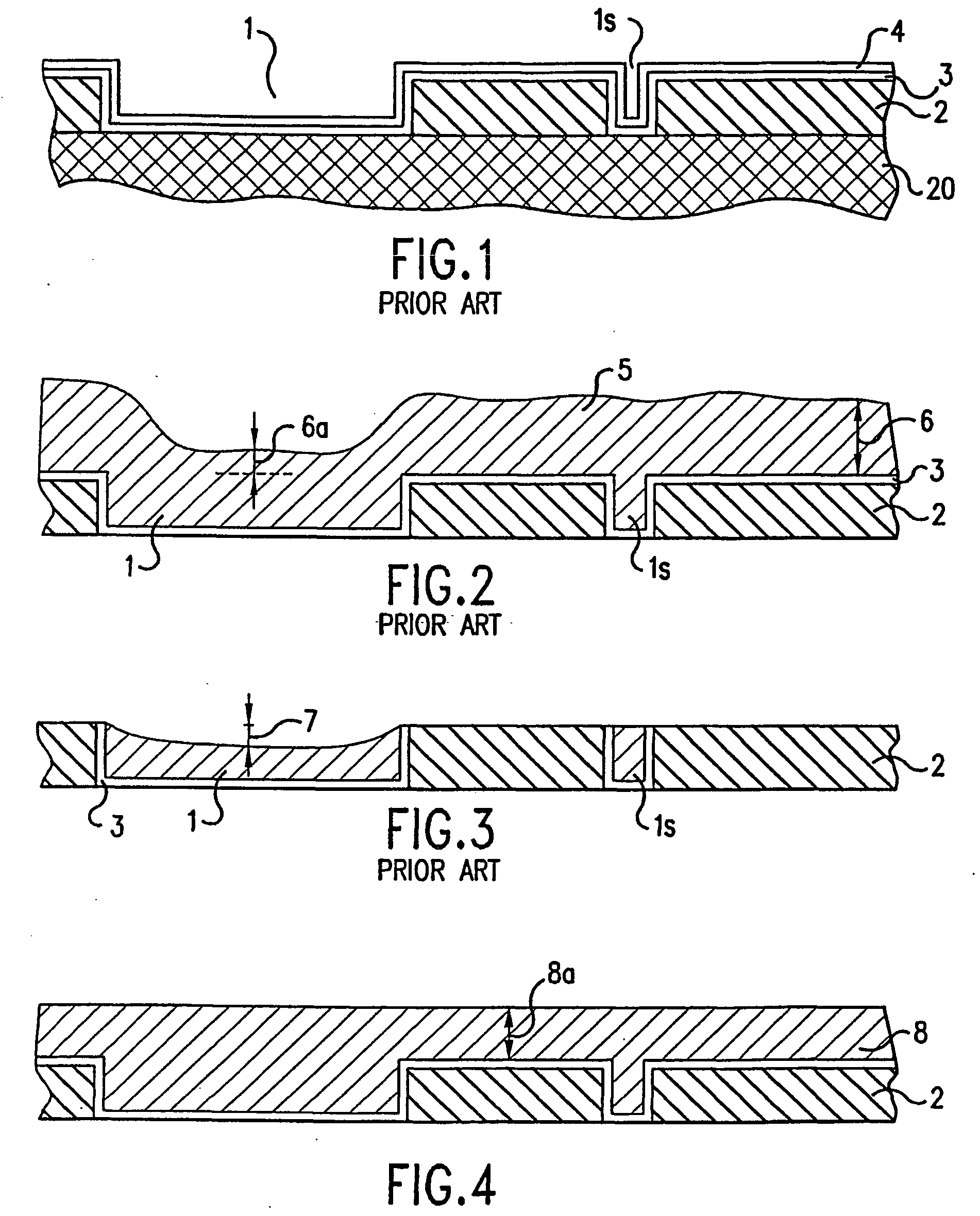
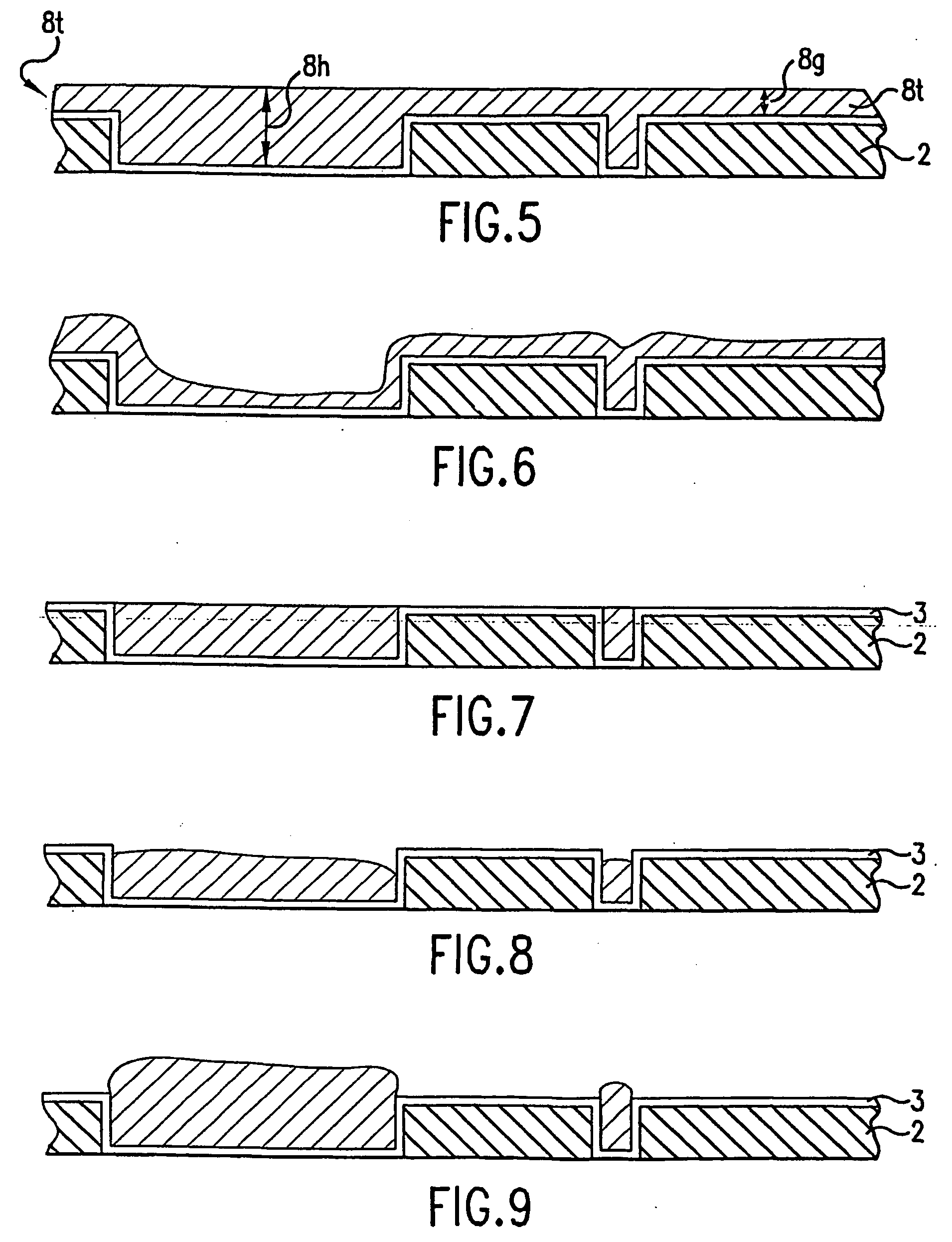
[0045] Five ml per liter of butyl-nitrite were added as a modifying agent to the electrolyte of Example 1 and the plating and polishing experiment of Example 2 was repeated using this modified plating solution. The resulting Cu deposit was highly planar and was similar to the structure shown in FIG. 4. Copper layer resistivity was still below 2×10⁻⁶ ohm-cm, demonstrating the ability of the modified electrolyte to yield high quality Cu deposits. The copper film was planar with uniform overburden over the sub-micron size features as well as the large features.

[0046] An anode assembly is disclosed in co-pending U.S. patent application Ser. No. 09 / 568,584, filed May 11, 2000, titled ANODE ASSEMBLY FOR PLATING AND PLANARIZING A CONDUCTIVE LAYER. A substrate holder / head assembly design is provided by co-pending U.S. patent application Ser. No. 09 / 472,523, filed Dec. 27, 1999, titled WORK PIECE CARRIER HEAD FOR PLATING AND POLISHING. The disclosures of these ...


PUM


Abstract

A layer structure usable in manufacturing an integrated circuit is made, in a single apparatus, by a particular process in which a patterned substrate is provided. An electrolyte solution, out of which a conductive material can be plated under an applied potential, is supplied over a surface of the patterned substrate, and a potential is applied so as to deposit a film of the conductive material out of the electrolyte solution and over the surface of the patterned substrate. The film of conductive material is preferably polished as it is deposited. The conductive material is then removed from field regions of the patterned substrate, while deposits of the conductive material are left in features defined in the patterned substrate. The deposits of the conductive material are then electrically isolated, resulting in the layer structure.

Description

[0001] This application claims the priority of U.S. provisional application No. 60 / 198,371, filed Apr. 19, 2000, the disclosure of which is expressly incorporated by reference herein.BACKGROUND AND SUMMARY OF THE INVENTION [0002] Multi-level integrated circuit manufacturing requires many steps of metal or metal alloy and insulator film depositions followed by photoresist patterning and etching or other material removal operation. After photolithography and etching, the resulting wafer or substrate surface is non-planar and contains many features such as vias, lines or channels, test pads and bond pads. Often, these features need to be filled with a specific material such as a metal, and then the wafer topographic surface needs to be planarized, making it ready for the next level of processing. [0003] Electrodeposition is a widely accepted technique for depositing a highly conductive material such as copper (Cu) into the features on the semiconductor wafer surface. Chemical mechanica...

Claims


Application Information

Patent Timeline
IPC IPC(8): C25D5/02
CPCC25D5/022C25D5/18C25D5/22H01L21/2885H01L21/32125H01L21/7684H01L21/76877C25D7/123C25D5/605
Inventor BASOL, BULENT M.UZOH, CYPRIAN E.TALIEH, HOMAYOUN
Owner NOVELLUS SYSTEMS
Why Eureka
Try Eureka