

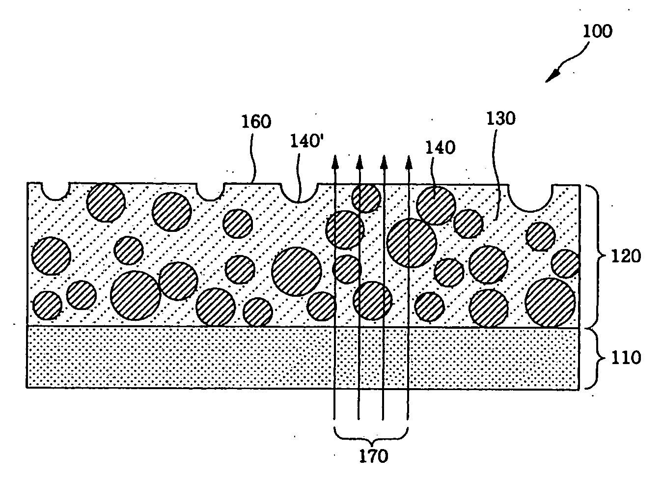
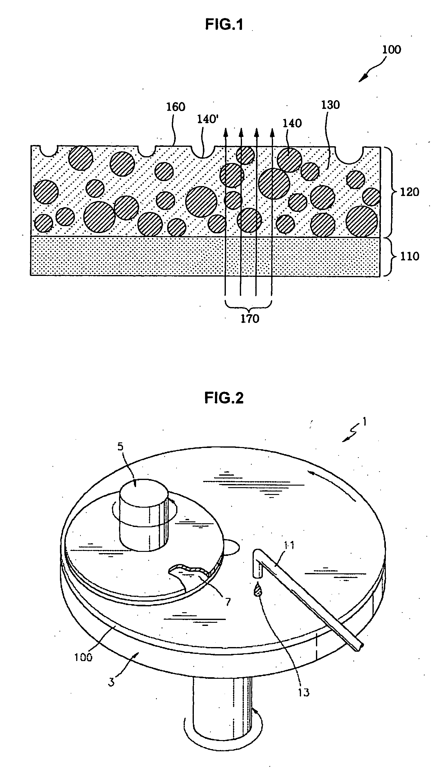
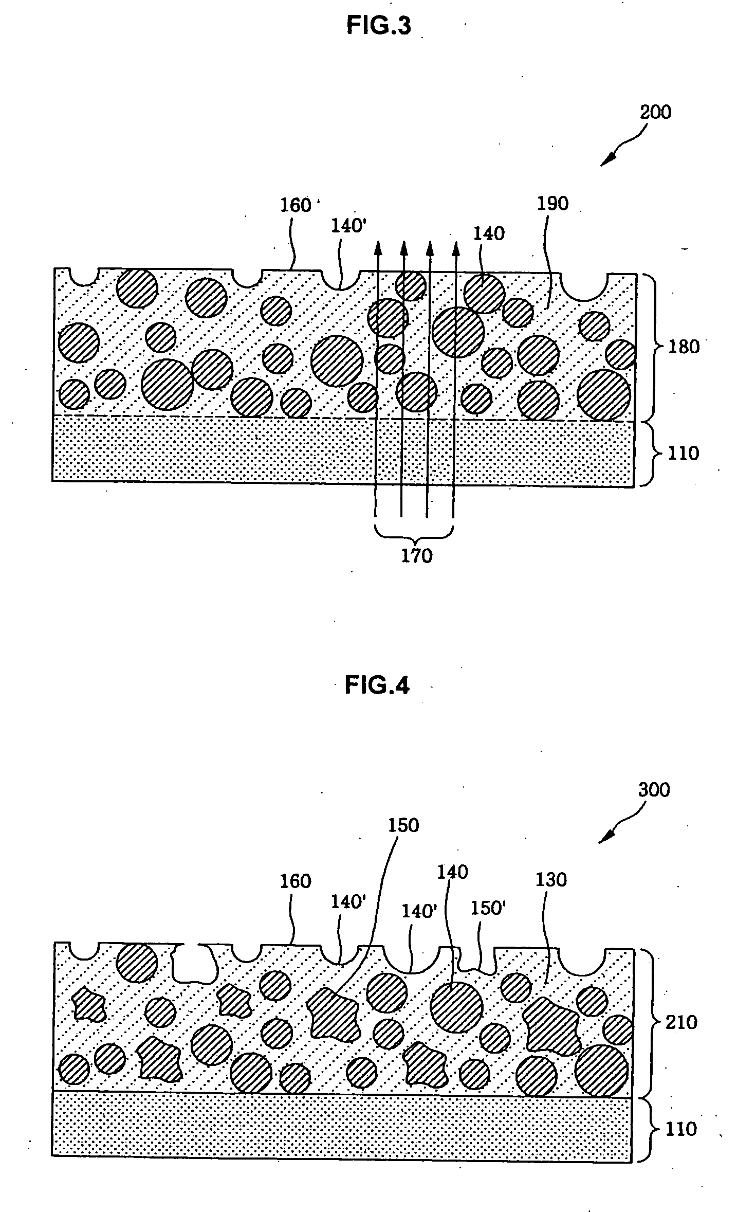
Polishing pad containing embedded liquid microelements and method of manufacturing the same
a technology of embedded liquid microelement and polishing pad, which is applied in the field of polishing pads, can solve the problems of uneven polishing on the surface surface scratches on the wafer during the polishing operation, and inability to maintain the polishing performance of the polishing pad constant, and achieve uniform abrasion and high precision. , the effect of maintaining the polishing performan
- Summary
- Abstract
- Description
- Claims
- Application Information
AI Technical Summary
Benefits of technology
Problems solved by technology
Method used
Image

Examples
experimental example 1
[0065] 100 g of a polyether-based isocyanate prepolymer (having an NCO content of 11%), 46 g of mineral oil (hereinafter, referred to as KF-70 (Seojin Chemical)), 5 g of nonylphenol ethoxylate (hereinafter, referred to as NP-2 (Korea Polyol)), and 33 g of MOCA were mixed at room temperature and then immediately poured into a mold. Then, gelling was performed for 30 minutes, and thereafter, curing was performed in an oven for 20 hours at 100° C. The cured product was taken out of the mold and cut to form a polishing layer of a polishing pad. A scanning electron microscope (SEM) photograph of a surface of the resultant polishing layer is shown in FIG. 6. It was detected from FIG. 6 that open pores having an average diameter of 10-30 μm existed on the surface of the polishing layer.
[0066] As a comparison example, according to a method of manufacturing a polishing pad disclosed in. U.S. Pat. No. 5,578,362, a polishing layer was manufactured using 100 g of a polyether-based isocyanate p...
experimental example 2
[0067] A polishing layer of a polishing pad was manufactured in the same manner as used in Experimental Example 1, with the exception that 40 g of KF-70 was used. A SEM photograph of the resultant polishing layer is shown in FIG. 8. It was detected from FIG. 8 that open pores having an average diameter of 30-40 μm existed on a surface of the polishing layer.
experimental example 3
[0068] A polishing layer of a polishing pad was manufactured in the same manner as used in Experimental Example 1, with the exception that 53 g of KF-70 was used. A SEM photograph of the resultant polishing layer is shown in FIG. 9. It was detected from FIG. 9 that open pores having an average diameter of 5-15 μm existed on a surface of the polishing layer.
PUM
| Property | Measurement | Unit |
|---|---|---|
| diameter | aaaaa | aaaaa |
| weight percent | aaaaa | aaaaa |
| diameter | aaaaa | aaaaa |
Abstract
Description
Claims
Application Information