Film formation method

a film and formation method technology, applied in the field of film formation methods, can solve the problems of difficult formation of tisisub>2 /sub>film consisting mainly of tisisub>2 /sub>crystals less uniform in grain size, and achieve good interface morphology

Inactive Publication Date: 2006-06-15
TOKYO ELECTRON LTD
View PDF11 Cites 21 Cited by
  • Summary
  • Abstract
  • Description
  • Claims
  • Application Information

AI Technical Summary

Benefits of technology

[0017] The present invention has been made in consideration of the problems described above, and has an object to provide a film formation method for forming a metal silicide film, such as a titanium silicide film, having a resistivity lower than that obtained by the conventional technique, without increasing the film formation temperature, where the metal silicide film is formed on an Si-containing portion of an target objec...

Problems solved by technology

However, as devices are more miniaturized, the depth of, e.g., Si diffusion layers is smaller, which makes it difficult for a TiSi2 film formed by conventional Ti-CVD methods to satisfy a required contact resistance.
In this case, conventional Ti-CVD methods require the use of a high process temperature, which makes it difficult to form a TiSi2 film consisting mainly of TiSi2 of the C54 crystal structure.
Further, as described above, where conventional plasma CVD methods are used to form a Ti film, TiSi2 crystals less uniform in grain size tend to...

Method used


Image

  • Film formation method
  • Film formation method
  • Film formation method

Examples


first embodiment

(1) Experiment for First Embodiment

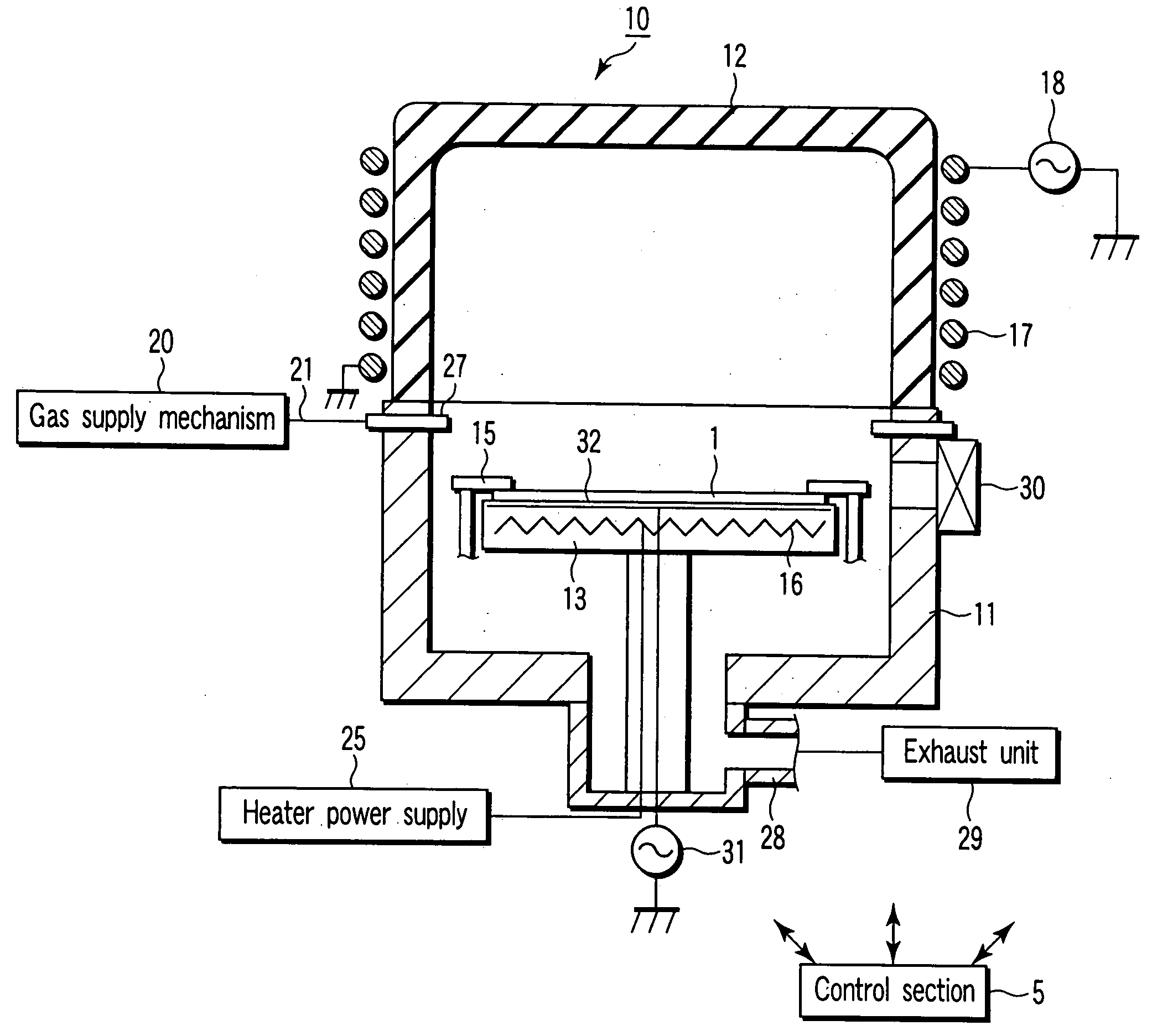
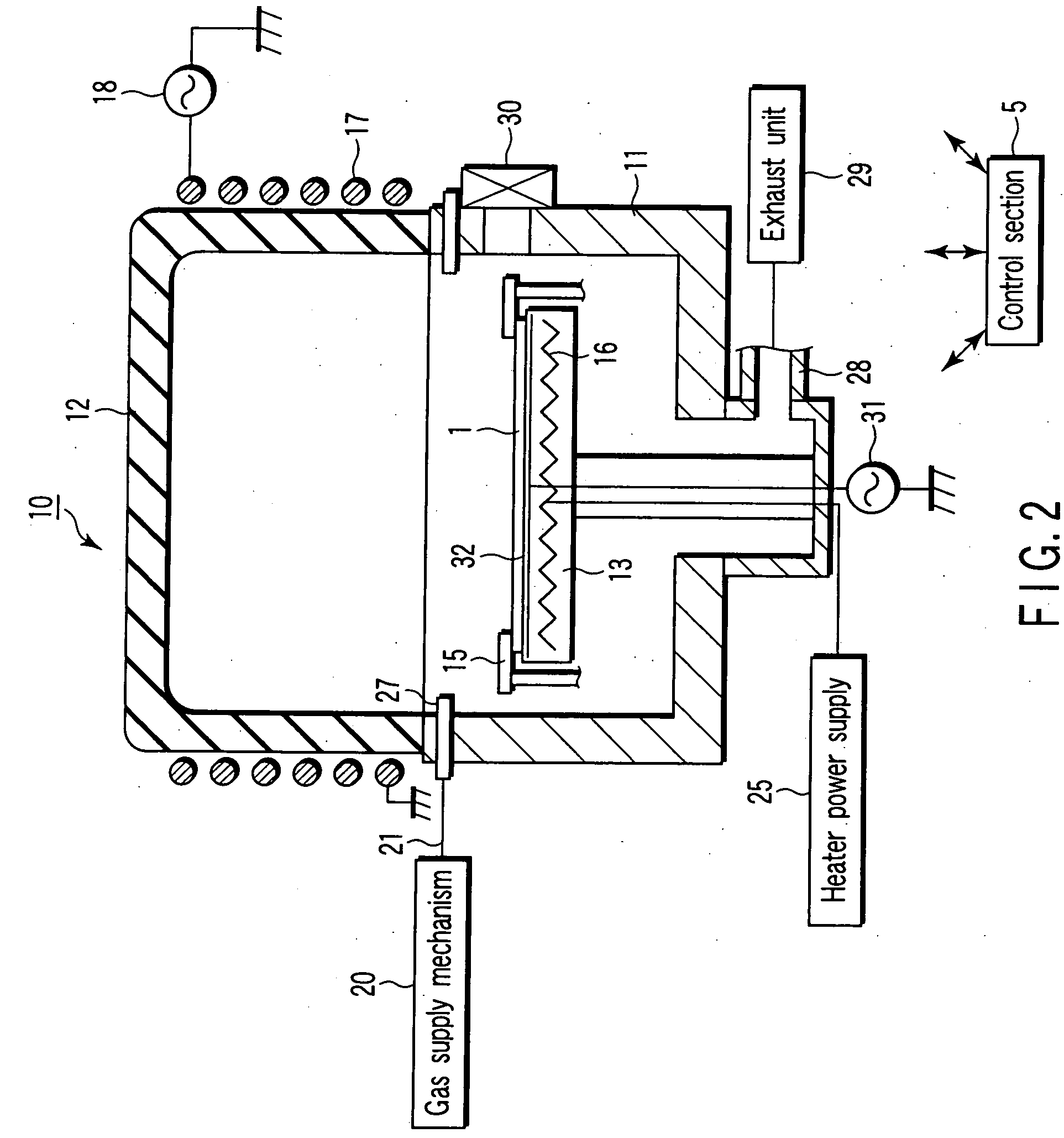
[0105] In this experiment, a plasma process using an RF was first performed on an Si wafer surface in the apparatus shown in FIG. 2. As regards the conditions of the process, the RF power supply 18 was set at a power level of 500W, the RF power supply 31 for bias was set at a power level of 800W to form Vdc at −530V. Thereafter, using the apparatus shown in FIG. 3, a process was performed for 31 seconds to form a TiSi2 film having a thickness of 43 nm, while the susceptor temperature was set at 640° C., and the wafer temperature was set at 620° C.

[0106]FIG. 8 shows an X-ray diffraction profile obtained in this experiment. As shown in FIG. 8, the TiSi2 film formed in accordance with the first embodiment rendered a high peak intensity of TiSi2 of the C54 crystal structure, wherein C54 formation of about 70% was confirmed.

[0107]FIG. 9 shows an SEM image of a cross section of this sample at a hole portion. The image of FIG. 9 shows a state after etch...

second embodiment

(2) Experiment for Second Embodiment

[0108] In this experiment, natural oxide films were removed in the apparatus shown in FIG. 2. Thereafter, a TiSi2 film is formed in the apparatus shown in FIG. 3, while TiCl4 was supplied for 10 seconds prior to plasma generation. A process was performed for 20 seconds to form a TiSi2 film having a thickness of 27 nm, while the susceptor temperature was set at 640° C., and the wafer temperature was set at 620° C.

[0109]FIG. 10 shows an X-ray diffraction profile obtained in this experiment. As shown in FIG. 10, a peak of TiSi2 of the C54 crystal structure was observed, and thus C54 formation was confirmed.

[0110]FIG. 11 shows an SEM image of a cross section of this sample at a hole portion. The image of FIG. 11 shows a state after etching was performed with hydrofluoric acid to remove the TiSi2 film by the etching. As shown in FIG. 11, the portion where the TiSi2 film was present was thin and uniform, so it is estimated that the crystal grain size ...


PUM

PropertyMeasurementUnit
Temperatureaaaaaaaaaa
Timeaaaaaaaaaa
Flow rateaaaaaaaaaa

Abstract

A titanium silicide film is formed on an Si wafer. At first, a plasma process using an RF is performed on the Si wafer. Then, a Ti-containing source gas is supplied onto the Si wafer processed by the plasma process and plasma is generated to form a Ti film. At this time, the Ti silicide film is formed by a reaction of the Ti film with Si of the Si wafer. The plasma process is performed on the Si wafer while the Si wafer is supplied with a DC bias voltage having an absolute value of 200V or more.

Description

CROSS-REFERENCE TO RELATED APPLICATIONS [0001] This is a Continuation-in-Part Application of PCT Application No. PCT / JP2004 / 007554, filed May 26, 2004, which was published under PCT Article 21(2) in Japanese. [0002] This application is based upon and claims the benefit of priority from prior Japanese Patent Application No. 2003-291667, filed Aug. 11, 2003, the entire contents of which are incorporated herein by reference. BACKGROUND OF THE INVENTION [0003] 1. Field of the Invention [0004] The present invention relates to a film formation method for performing a plasma process on a target object, such as an Si-containing portion, e.g., an Si-substrate surface or metal silicide layer to form a metal silicide film. [0005] 2. Description of the Related Art [0006] In recent years, multi-layered interconnection structures are being increasingly used for circuitry, because higher density and higher integration degree are required in manufacturing semiconductor devices. Under the circumstan...

Claims


Application Information

Patent Timeline
IPC IPC(8): H05H1/24C23C16/08C23C16/56H01L21/285
CPCC23C16/08C23C16/56H01L21/28518H01L21/285C23C16/42
Inventor MURAKAMI, SEISHIMORISHIMA, MASATONARUSHIMA, KENSAKU
Owner TOKYO ELECTRON LTD
Why Eureka
Try Eureka