Plasma cleaning of deposition chamber residues using duo-step wafer-less auto clean method

a technology of auto clean and deposition chamber, which is applied in the direction of cleaning using liquids, coatings, chemistry apparatus and processes, etc., can solve the problems of undesired residues, defective substrates, and unsuitable residues deposited on the inner surfaces of the process,

Inactive Publication Date: 2006-06-22
LAM RES CORP
View PDF6 Cites 27 Cited by
  • Summary
  • Abstract
  • Description
  • Claims
  • Application Information

AI Technical Summary

Problems solved by technology

Although care and caution is involved during the monitoring of a chemical process, more often than not, undesired residues are deposited on the inner surfaces of the process chambers where the processes are taking place.
The undesired residues, unfortunately, get deposited in and around the walls of the processing chamber.
The build up of residues inside the processing chamber, over time, not only make the processes unreliable and shifted from baseline, but also result in degraded, defective substrates in the form of defects.
In addition, process etch rates or deposition rates can vary over time due to the changing chamber conditions from residue build-up resulting in out of control process performance.
Unfortunately, such cleaning operations affect a substrate processing system's utilization in a variety of ways.
When a wet clean is performed, opening the processing chamber and physically wiping the chamber's interior surfaces results in even more downtime because the processing environment must subsequently be re-stabilized.
Although such a recipe has the advantage that the number of process steps can be reduced or not, it fails to ensure complete removal of different byproducts, such as carbon based organic residues and semiconductor based silicon residues.
In fact, the removal rates for silicon and carbon deposition are in opposition to each other.
As both fluorine-based and oxygen-based chemistries are mixed together, the removal rates of both silicon and carbon are not at optimal levels.
Thus, the one step approach can not yield optimized removal rates for silicon and carbon deposition.
When a composite WAC recipe for both silicon and carbon byproduct removal is used involving a specific mixture of separate etchant gases for silicon removal and for carbon removal, it suffers from non-optimized lower removal rates of both silicon and carbon-based deposition byproducts.
That is, the one step composite WAC approach is not tuned to achieve complete by-product removal of both the silicon and the carbon by-products.
In effect, the one step composite WAC approach compromises the effectiveness of the removal of the byproducts for the convenience of using a single all-encompassing WAC chemistry.
Consequently, the chamber will be under-cleaned which results in a build up of material, or the chamber will be over-cleaned which results in the degradation of chamber parts and a shortening of their lifetime.
The build up of these compounds causes variability of the plasma processing operations performed in the processing chamber.
Another shortcoming of frequent cleaning operations is that they tend to increase wear on the processing chamber components when over-cleaning occurs resulting in decreased lifetime of the components.
In turn, the cost of consumables increases.

Method used


Image

  • Plasma cleaning of deposition chamber residues using duo-step wafer-less auto clean method
  • Plasma cleaning of deposition chamber residues using duo-step wafer-less auto clean method
  • Plasma cleaning of deposition chamber residues using duo-step wafer-less auto clean method

Examples


Embodiment Construction

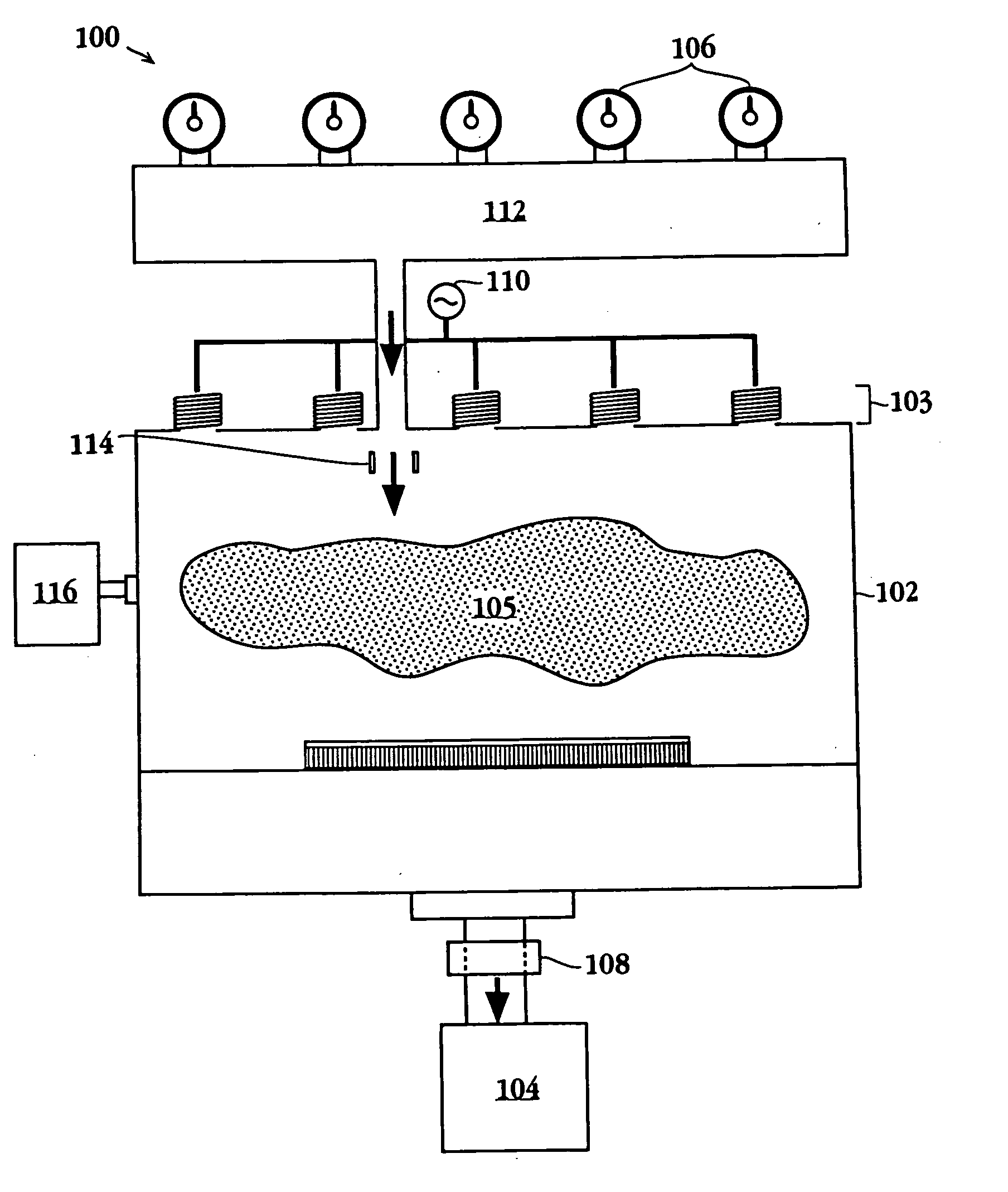
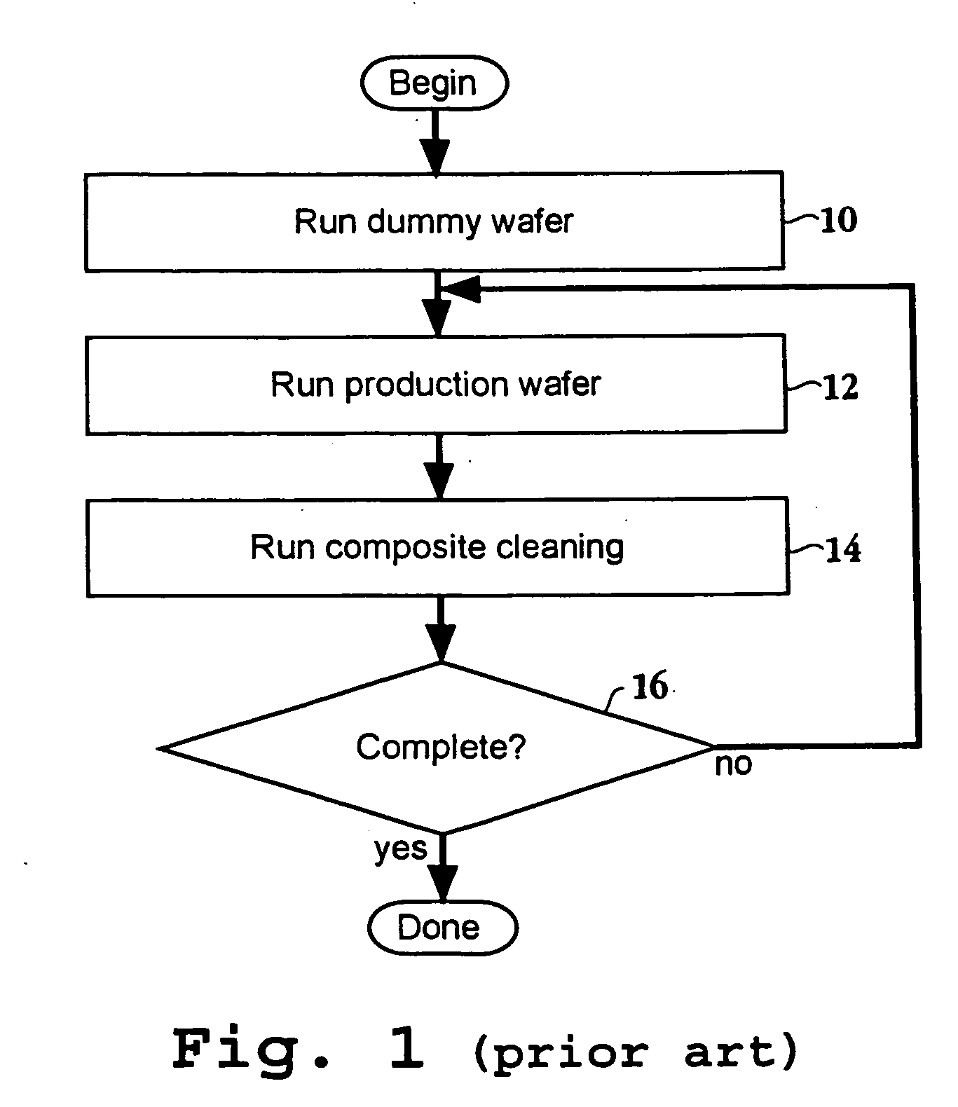
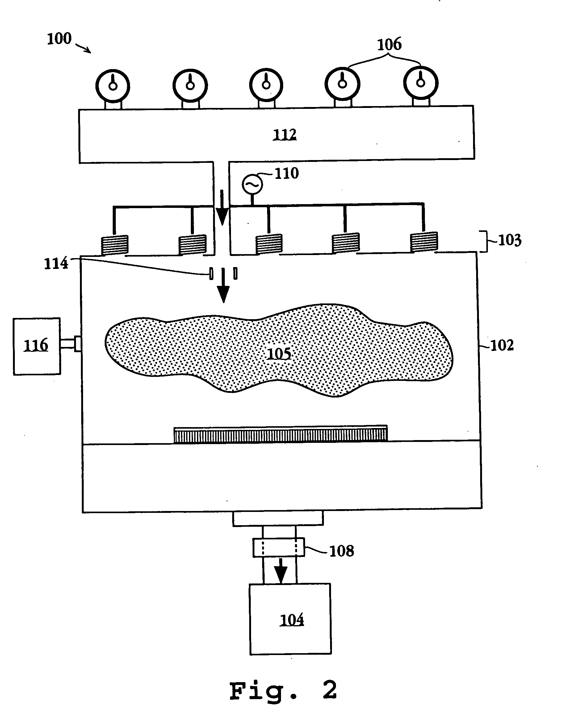
[0029] An invention is described for providing an optimized dual step wafer-less auto clean method optimized for removing multiple byproducts deposited onto walls of a semiconductor processing chamber. It will be obvious, however, to one skilled in the art, that the present invention may be practiced without some or all of these specific details. In other instances, well known process operations have not been described in detail in order not to obscure the present invention. FIG. 1 is described in the “Background of the Invention” section.

[0030] The basic concept of plasma etching is rather direct. A glow discharge is utilized to produce chemically reactive species (neutral atoms, radicals and ions) from a relatively inert molecular gas. The etching gas is selected so as to generate species that react chemically with the material to be etched, and whose reaction product with the etched material is volatile so that it can be removed from the processing chamber.

[0031] An ideal dry e...


PUM

PropertyMeasurementUnit
pressureaaaaaaaaaa
pressureaaaaaaaaaa
poweraaaaaaaaaa

Abstract

A method involving plasma cleaning of deposit residues in process chamber using duo-step wafer-less auto clean method is detailed. Specifically, the method involves cleaning the processing chamber by flowing a first gaseous composition with at least about 75% of fluorine-containing compound of the formula XyFz, into a processing chamber and then forming a first etchant plasma which removes silicon and silicon based byproducts from the interior surfaces of the processing chamber. The method then involves flowing a second gaseous composition into the processing chamber with a composition of at least about 50% O2 and forming a plasma from the second gaseous composition to provide a second etchant plasma which removes carbon and carbon based byproducts from the interior surfaces of the processing chamber. A system configured to execute the two step cleaning process is also provided.

Description

CROSS REFERENCE TO RELATED APPLICATIONS [0001] This application claims priority from U.S. application Ser. No. 10 / 139,042 which claims priority to U.S. Provisional Patent Application Ser. No. 60 / 288,678 filed May 4, 2001 and entitled “Plasma Cleaning of Deposition Chamber Residues Using Duo-Step Wafer-Less Auto Clean Method.” These applications are herein incorporated by reference. This application is related to (1) U.S. patent application Ser. No. 10 / 138,980, filed on May 3, 2002, and entitled “Endpoint Determination of Process Residues in Wafer-less Auto Clean Process Using Optical Emission Spectroscopy,” (2) U.S. patent application Ser. No. 10 / 138,288, filed May 2, 2002, and entitled “High Pressure Wafer-less Auto Clean for Etch Applications”. These applications are hereby incorporated by reference.FIELD OF THE INVENTION [0002] This invention generally relates to an apparatus and method of cleaning a processing chamber to remove previously deposited chamber residues, which have a...

Claims


Application Information

Patent Timeline
Patent Type & Authority Applications(United States)
IPC IPC(8): B08B6/00B08B3/06B08B7/00C23C16/44H01J37/32
CPCB08B3/06B08B7/0035C23C16/4405H01J37/32862H01J37/32935H01J37/32963Y10S438/905H01L21/3065
Inventor RICHARDSON, BRETT C.WONG, VINCENT
Owner LAM RES CORP
Why Eureka
Try Eureka