Phosphorescent oleds with exciton blocking layer

a technology of exciton blocking layer and phosphorescent oled, which is applied in the direction of discharge tube luminescnet screen, natural mineral layered product, etc., can solve the problems of large loss of efficiency, large excitons created, and performance limitations that have been a barrier to many desirable applications, so as to reduce the drive voltage and improve efficiency.

Active Publication Date: 2006-06-22
GLOBAL OLED TECH
View PDF14 Cites 199 Cited by
  • Summary
  • Abstract
  • Description
  • Claims
  • Application Information

AI Technical Summary

Benefits of technology

[0017] The devices of the invention exhibit improved efficiency and reduced drive voltage.

Problems solved by technology

While organic electroluminescent (EL) devices have been known for over two decades, their performance limitations have represented a barrier to many desirable applications.
However, only 25% of the excitons created in an EL device are singlet excitons.
This results in a large loss in efficiency since 75% of the excitons are not used in the light emission process.
rity. However, in this case, blue OLED devices employing these disclosed materials require use of substantial amounts of the phosphorescent emitters and still do not solve the high voltage pr
The document describes that devices utilizing plural host compounds show higher current and higher efficiencies at a given voltage; however, reported luminance data are quite moderate.
However, use of these materials alone does not give the optimum performance possible in an electroluminescent device.

Method used


Image

  • Phosphorescent oleds with exciton blocking layer
  • Phosphorescent oleds with exciton blocking layer
  • Phosphorescent oleds with exciton blocking layer

Examples


examples 1-4

DEVICE EXAMPLES 1-4

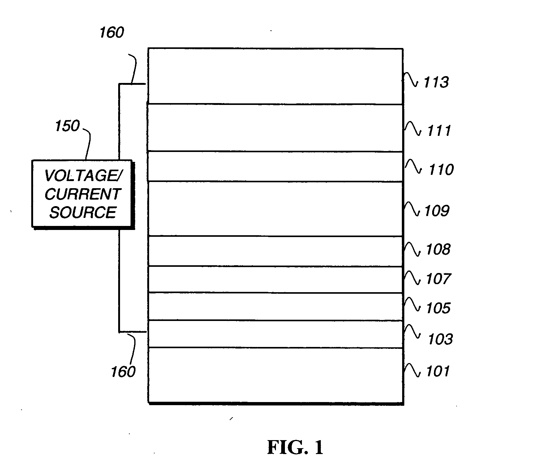
[0365] An EL device (Device 1) satisfying the requirements of the invention was constructed in the following manner: [0366] 1. A glass substrate, coated with an approximately 85 nm layer of indium-tin oxide (ITO) as the anode, was sequentially ultrasonicated in a commercial detergent, rinsed in deionized water, degreased in toluene vapor and exposed to oxygen plasma for about 1 minute. [0367] 2. Over the ITO was deposited a 1 nm fluorocarbon (CFx) hole injecting layer (HIL) by plasma-assisted deposition of CHF3. [0368] 3. A hole transporting layer (HTL) of N,N′-di-1-naphthyl-N,N′-diphenyl-4,4′-diaminobiphenyl (NPB) having a thickness of 37.5 nm was then evaporated from a resistively heated tantalum boat. [0369] 4. An exciton blocking layer (EBL) of 4,4′,4″-tris(carbazolyl)-triphenylamine (TCTA) having a thickness of 37.5 nm was then evaporated from a resistively heated tantalum boat. [0370] 5. A 35 nm light emitting layer (LEL) consisting of a mixture of 2,2′,2″-(...

examples 5-6

DEVICE EXAMPLES 5-6

[0382] An EL device (Device 5) satisfying the requirements of the invention was fabricated in an identical manner to Device 1 except that about 1 wt. % of lithium was co-deposited with the electron transporting Alq material.

[0383] An EL device (Device 6) also satisfying the requirements of the invention was fabricated in an identical manner to Device 5 except that the Alq layer did not contain lithium.

[0384] The devices were operated at a constant current density of 1 mA / cm2, and voltage and luminance properties were measured. The results are shown in Table 2.

TABLE 2Evaluation Results for EL devices 5 and 6.LuminousyieldVoltageDevice(cd / A)(V)CIExCIEyType551.66.40.340.30Invention650.09.20.330.30Invention

[0385] The results in Table 2 comparing Devices 5 and 6 show that in the practice of the invention, the incorporation of the alkali metal dopant lithium into the electron transporting layer further decreases the drive voltage.

examples 7-8

DEVICE EXAMPLES 7-8

[0386] A EL device (Device 7) satisfying the requirements of the invention was fabricated in an identical manner to Device 1 except that an NPB layer was not deposited, and a 75 nm exciton blocking layer of 1,1-Bis(4-(N,N-di-p-tolylamino)phenyl)cyclohexane (TAPC) was deposited in place of the 37.5 nm layer of TCTA. TAPC is also used in place of TCTA in the LEL at a concentration of 20 wt. % of the total of the co-hosts. Therefore, Device 7 has the following structure of layers: ITO|CFx (1 nm)|TAPC (75 nm)|(TPBI+20 wt. % TAPC)+6 wt. % Ir(ppy)3 (35 nm)|TPBI (10 nm)|Alq (40 nm)|Mg:Ag (220 nm).

[0387] A comparative EL device (Device 8) not satisfying the requirements of the invention was fabricated in an identical manner to Device 7 except TAPC was not included in the LEL and TPBI was used as a neat host for Ir(ppy)3.

[0388] These devices were operated at a constant current density of 1 mA / cm2, and voltage and luminance properties were measured. The results are shown ...


PUM

PropertyMeasurementUnit
triplet energyaaaaaaaaaa
thickaaaaaaaaaa
operating voltagesaaaaaaaaaa

Abstract

An electroluminescent device comprises a cathode and an anode; and, located therebetween, a light-emitting layer (LEL) comprising at least one hole transporting co-host and at least one electron transporting co-host, together with at least one phosphorescent emitter, and wherein the triplet energy of each of the co-host materials is greater than the triplet energy of the phosphorescent emitter, and further containing an exciton blocking layer comprising a hole transporting material with triplet energy greater or equal to 2.5 eV adjacent the emitting layer on the anode side. The invention provides devices that emit light with high luminous efficiency at low voltage.

Description

CROSS REFERENCE TO RELATED APPLICATION [0001] This application is being co-filed with an application entitled “Organometallic Materials And Electroluminescent Devices”, under Attorney Docket No. 88692, the contents of which are incorporated herein by reference. FIELD OF THE INVENTION [0002] This invention relates to an organic light emitting diode (OLED) electroluminescent (EL) device comprising an exciton blocking layer and a light emitting layer including hole- and electron transporting materials, together with a phosphorescent emitter, that can provide desirable electroluminescent properties such as high luminous and power efficiencies and low operational voltage. BACKGROUND OF THE INVENTION [0003] While organic electroluminescent (EL) devices have been known for over two decades, their performance limitations have represented a barrier to many desirable applications. In simplest form, an organic EL device is comprised of an anode for hole injection, a cathode for electron inject...

Claims


Application Information

Patent Timeline
Patent Type & Authority Applications(United States)
IPC IPC(8): H01L51/54H05B33/14
CPCC09K11/06C09K2211/1007C09K2211/1014C09K2211/1022C09K2211/1044C09K2211/1059C09K2211/1074C09K2211/1077C09K2211/185H01L51/0054H01L51/0059H01L51/0067H01L51/0069H01L51/007H01L51/0085H01L51/0087H01L51/5016Y10S428/917H10K85/622H10K85/656H10K85/631H10K85/6565H10K85/654H10K85/346H10K85/342H10K50/11H10K2101/10
Inventor KONDAKOVA, MARINA E.DEATON, JOSEPH C.BROWN, CHRISTOPHER T.KLUBEK, KEVIN P.HUO, SHOUQUAN
Owner GLOBAL OLED TECH
Why Eureka
Try Eureka