

Photoelectric conversion device
a conversion device and photoelectric technology, applied in the field of photoelectric conversion devices, can solve the problems of reducing the efficiency of photoelectric conversion, no longer working as a device, and significantly deteriorating the characteristics of photoelectric conversion, and achieves the effects of low cost, large roughness factor, and large short circuit current density
- Summary
- Abstract
- Description
- Claims
- Application Information
AI Technical Summary
Benefits of technology
Problems solved by technology
Method used
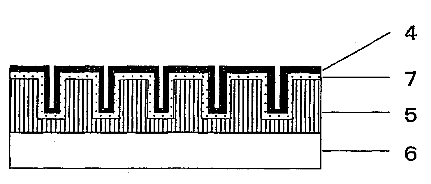
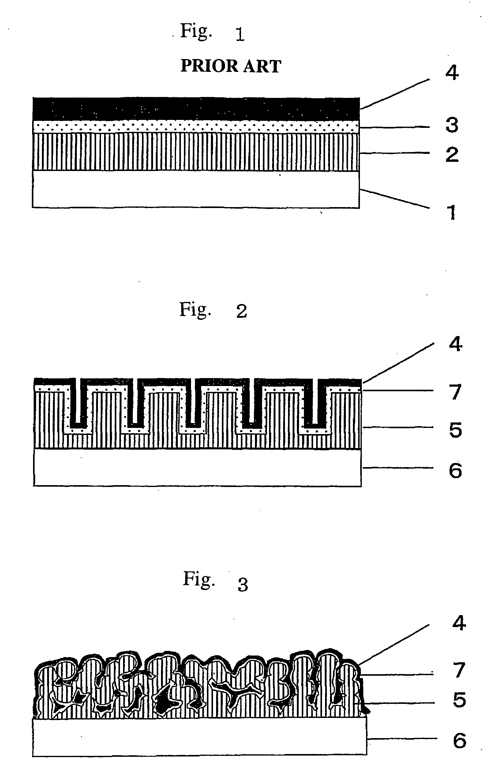
Image

Examples
example 1
[0064] A dye sensitizing photoelectric conversion device according to the present invention was manufactured by the following procedures. First of all, a titanium substrate with a size of 5×5 cm and a thickness of 1 mm was prepared and masked on its one surface with an epoxy resin. The titanium substrate was electrolytic polished using a methanol-sulfuric acid mixed solution to planish the other surface. After the electrolytic polishing, the surface profile of the substrate was observed with an AFM (atomic force microscope) and it was confirmed that the substrate had a very smooth surface structure. The roughness factor of the substrate surface was 1.04.
[0065] Thereafter, the titanium substrate was anodized by applying a voltage of 10 V for 30 minutes in an aqueous electrolyte solution containing 0.5 mass % of hydrofluoric acid thereby forming a titanium oxide film on the substrate. The electrolyte solution was set at a temperature of 16° C.
[0066] Thereafter, the substrate with th...
example 2
[0070] A dye sensitizing photoelectric conversion device according to the present invention was manufactured by the following procedures. First of all, a titanium substrate with a size of 5×5 cm and a thickness of 1 mm was prepared and masked on its one surface with an epoxy resin. The titanium substrate was electrolytic polished using a methanol-sulfuric acid mixed solution to planish the other surface. After the electrolytic polishing, the surface profile of the substrate was observed with an AFM (atomic force microscope) and it was confirmed that the substrate had a very smooth surface structure. The roughness factor of the substrate surface was 1.04.
[0071] Thereafter, the titanium substrate was anodized by applying a voltage of 20 V for 20 minutes in an aqueous electrolyte solution containing 0.5 mass % of hydrofluoric acid thereby forming a titanium oxide film on the substrate. The electrolyte solution was set at a temperature of 16° C.
[0072] Thereafter, the substrate with th...
example 3
[0076] A dye sensitized photoelectric conversion device according to the present invention was manufactured by the following procedures. First of all, an ITO glass substrate with a size of 5×5 cm and a thickness of 3 mm was prepared, and titanium of a thickness of 1000 nm was laminated on the ITO by vacuum-deposition. The surface profile of the titanium was observed with an AFM (atomic force microscope) and it was confirmed that the titanium had a very smooth surface structure. The roughness factor of the titanium surface was 1.02.
[0077] Thereafter, the deposited titanium was anodized in an aqueous electrolyte solution containing 1.5 mol / l of sulfuric acid and 0.3 mol / l of hydrogen peroxide by constant-current electrolysis until the generated voltage reached at 150 V thereby forming a titanium oxide film on the substrate. The current density and the temperature of the electrolyte solution were set to 30 mA / cm2 and 16° C., respectively. The film thus obtained was a rutile type cryst...
PUM
 Abstract
Description
Claims
Application Information