Charged-particle beam exposure apparatus and method

Inactive Publication Date: 2006-06-29
CANON KK
View PDF3 Cites 16 Cited by
  • Summary
  • Abstract
  • Description
  • Claims
  • Application Information

AI Technical Summary

Benefits of technology

[0010] The present invention has been made in consideration of the above situation, and has as its object to provide a multibeam charged-particle beam exposure apparatus capable of mak

Problems solved by technology

The exposure apparatus has been considered to be unfit for mass-production until now because of a low throughput.
Unfortunately, in the stencil mask type charged-particle beam exposure apparatus, if the intensities of charged-particle beams which strike the stencil mask are nonuniform in the irradiation region, the pattern to be transferred will deform.
In particular, if a variation in intensities of charged-particle beams occurs due to a change in intensity distribution of the charged-particle beams during exposure, the drawing accuracy of the exposure apparatus greatly decreases.
However, irradiatio

Method used


Image

  • Charged-particle beam exposure apparatus and method
  • Charged-particle beam exposure apparatus and method
  • Charged-particle beam exposure apparatus and method

Examples


Example

First Embodiment

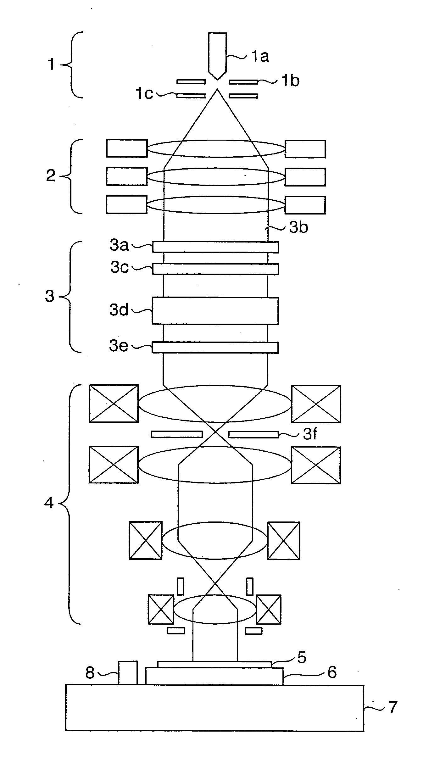
[0024]FIG. 1 is an elevation view schematically showing the main part of the multi-electron-beam exposure apparatus according to the present invention. An electron gun 1 includes a cathode 1a, grid 1b, and anode 1c. Electrons emitted by the cathode 1a form a crossover image between the grid 1b and anode 1c. The crossover image will be referred to as an electron source hereinafter.

[0025] An electron beam emitted by the electron source is collimated into an almost parallel electron beam by a collimator lens 2 including a plurality of electrostatic electron lenses. A correction electron optical system 3 is irradiated with almost the parallel electron beam.

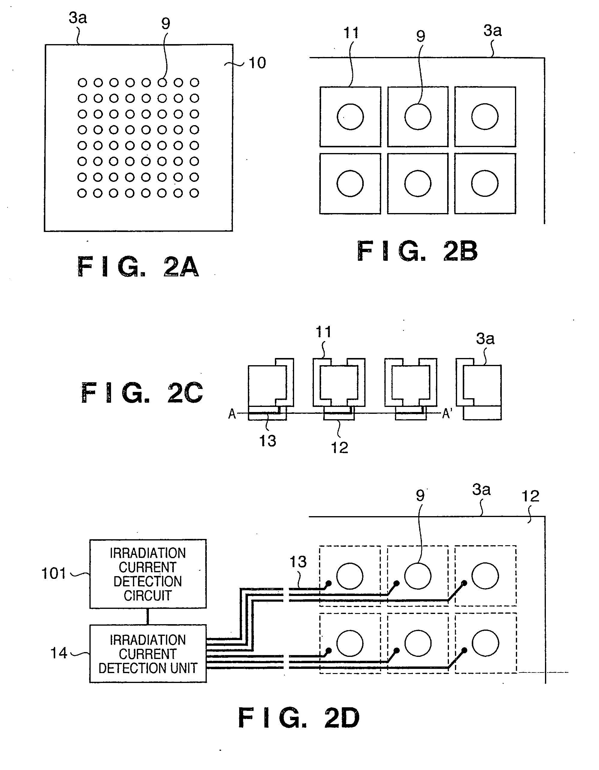
[0026] The correction electron optical system 3 comprises an aperture array 3a, a grid array 3c, an element electron optical system 3d, a blanker array 3e, and a stopper array 3f, which are arranged in turn from the electron gun 1 side along the optical axis. The aperture array 3a includes an irradiation current det...

Example

Second Embodiment

[0066] A semiconductor device manufacturing process using the exposure apparatus according to the first embodiment will be described as the second embodiment of the present invention. FIG. 9 is a flowchart showing the flow of the overall semiconductor device manufacturing process. In step 11 (circuit design), a semiconductor device circuit is designed. In step 12 (EB data conversion), exposure control data of the exposure apparatus is created on the basis of the designed circuit pattern.

[0067] In step 13 (wafer formation), a wafer is formed using a material such as silicon. In step 14 (wafer process) called a pre-process, an actual circuit is formed on the wafer by lithography using the wafer and the exposure apparatus which has received the prepared exposure control data. Step 15 (assembly) called a post-process is the step of forming a semiconductor chip by using the wafer formed in step 14. The post-process includes an assembly process (dicing and bonding) and ...


PUM


Abstract

This invention makes it possible to provide a charged-particle beam exposure apparatus which implements highly accurate pattern drawing by detecting the intensity distribution of irradiation charged-particle beams and controlling the distribution to be uniform. The charged-particle beam exposure apparatus splits a charged-particle beam irradiated from a charged-particle beam source into a plurality of charged-particle beams by a plurality of apertures formed in an aperture array (3a). The charged-particle beam exposure apparatus includes a detection unit which detects the intensity of the charged-particle beam passing through the aperture formed in the aperture array (3a), and a grid array which adjusts the intensity of the charged-particle beam on the basis of the detection result obtained by the detection unit. The charged-particle beam exposure apparatus makes the intensity distribution of the charged-particle beams which reach a wafer (5) through the plurality of apertures uniform.

Description

FIELD OF THE INVENTION [0001] The present invention relates to a charged-particle beam exposure apparatus and method. BACKGROUND OF THE INVENTION [0002] Recently, as a measure for implementing highly integrated and micropatterned semiconductor devices, an exposure apparatus using a charged-particle beam such as an electron beam has been developed. The exposure apparatus has been considered to be unfit for mass-production until now because of a low throughput. [0003] However, the exposure apparatus is becoming prospective to attain a practical throughput for mass-production by recent developments in a stencil mask type electron beam exposure apparatus and multi-electron-beam exposure apparatus. Since these exposure apparatuses have a wider area to be exposed at once, i.e., exposure area than that adopted in the prior art, a throughput can be increased. [0004] Unfortunately, in the stencil mask type charged-particle beam exposure apparatus, if the intensities of charged-particle beams...

Claims


Application Information

Patent Timeline
IPC IPC(8): G21K5/10
CPCB82Y10/00B82Y40/00H01J37/243H01J37/304H01J37/3177H01J2237/0453H01J2237/30472
Inventor MAEDA, TAKASHI
Owner CANON KK
Why Eureka
Try Eureka