
Non volatile semiconductor memory device

Active Publication Date: 2006-06-29
RENESAS ELECTRONICS CORP
View PDF3 Cites 4 Cited by
  • Summary
  • Abstract
  • Description
  • Claims
  • Application Information

AI Technical Summary

Benefits of technology

[0008] In view of the above situation, the object of the present invention is to provide a technology of allowing a nonvolatile semiconductor memory to increase the capacity without increasing the power supply circuits which are the peripheral circuits of the nonvolatile semiconductor memory.
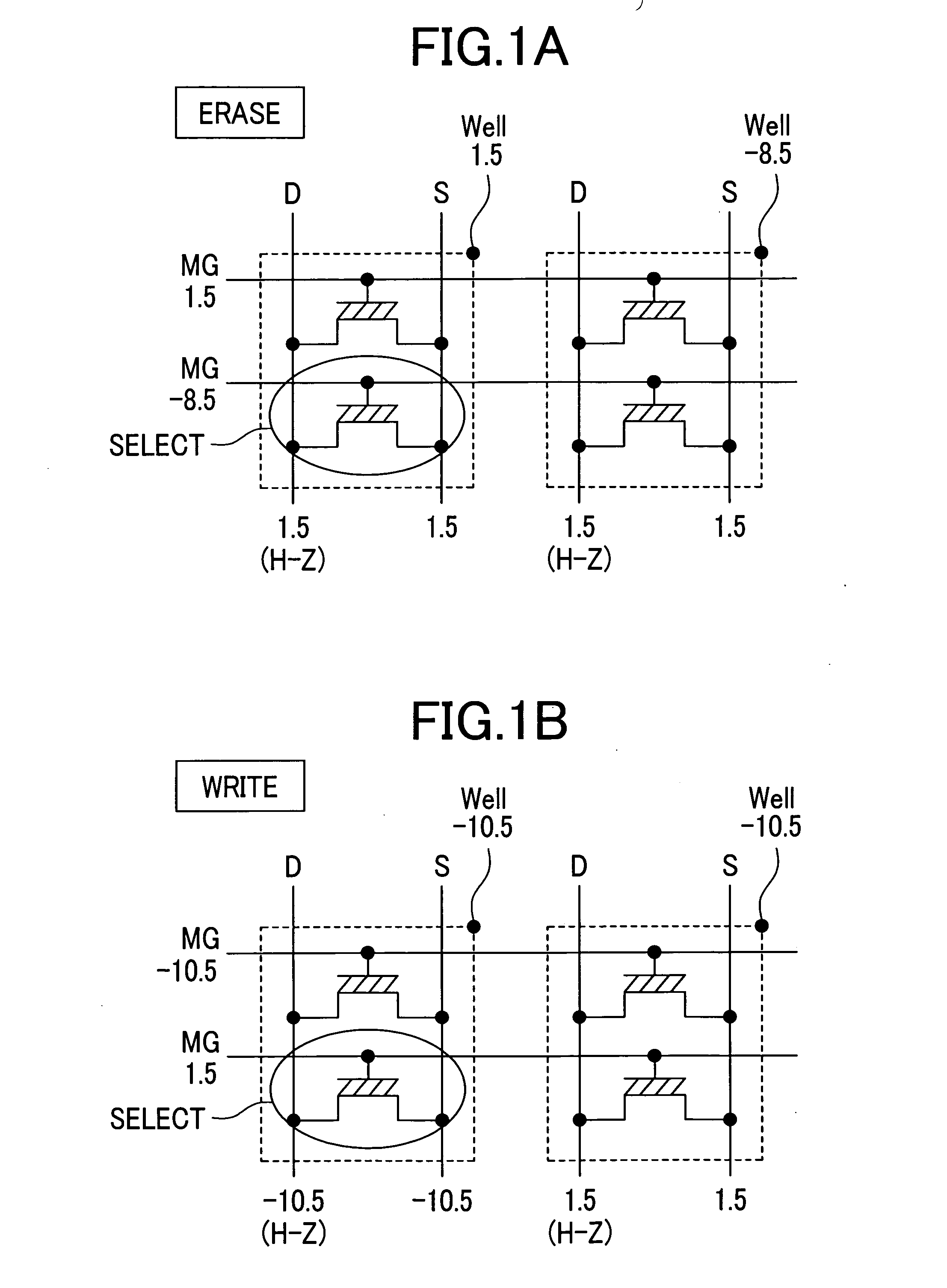
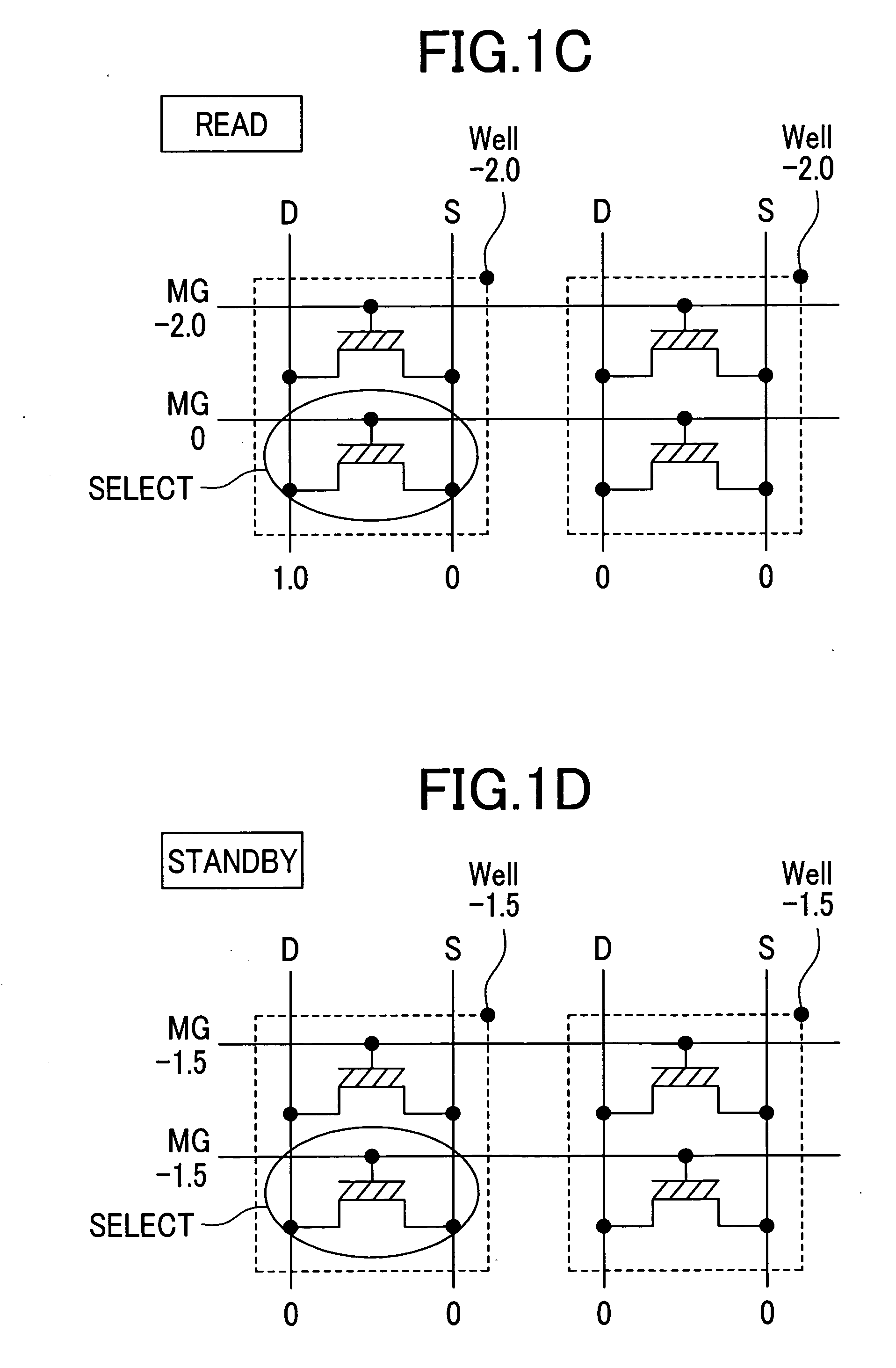
[0012] Thereby, at the time of erase or write, it is not necessary to supply high voltage to all the memory cell blocks and, at the time of read and standby, it is possible to maintain the linearity (carry out read without weighting memory cell brocks astride them) of the read by supplying high voltage to all the memory cell blocks.
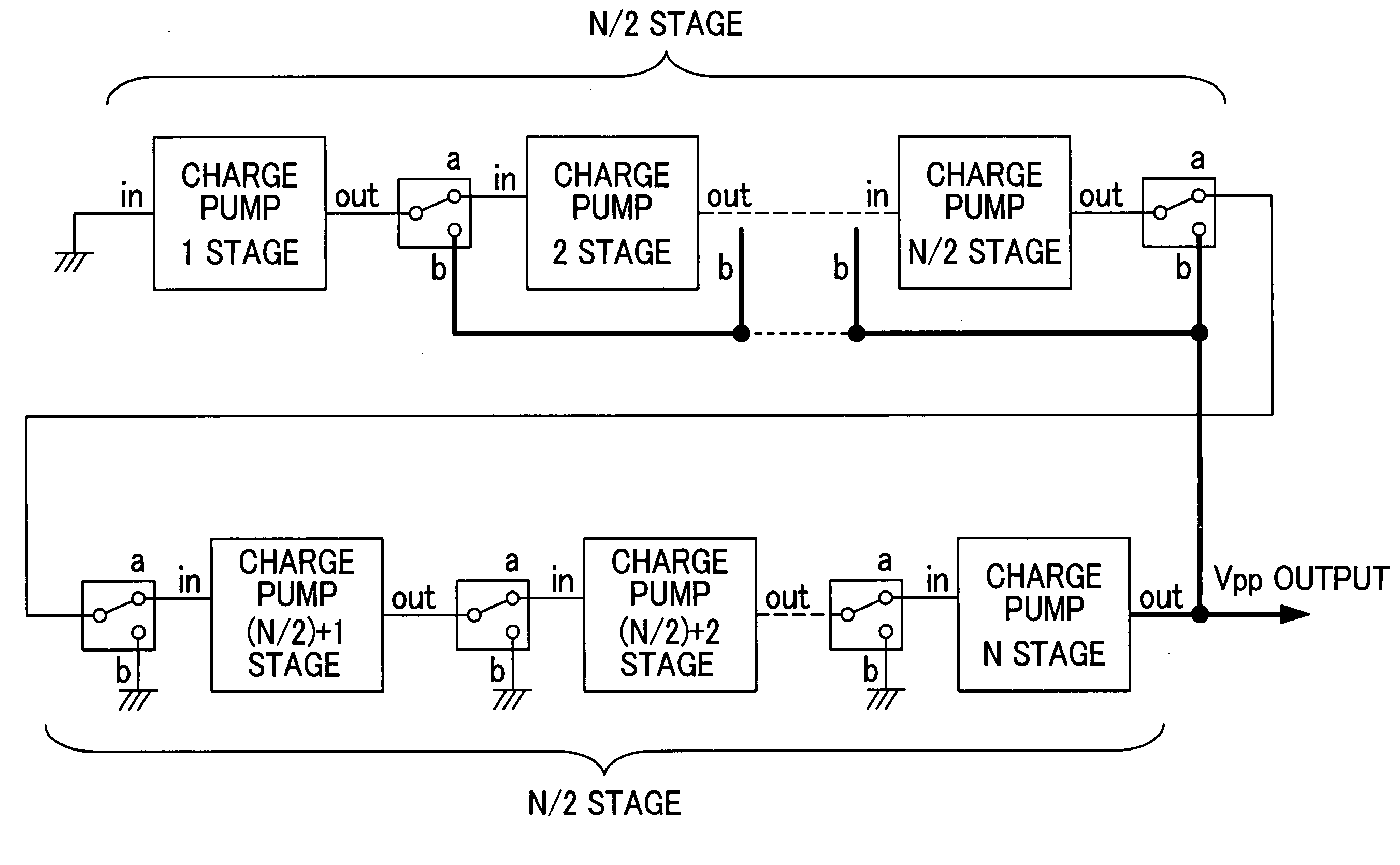
[0014] It is possible to carry out the erase and write of plural memory cell blocks by selecting memory cell blocks one by one in a power supply circuit containing a charge pump circuit having the capability of carrying out the erase and write of a memory cell block and, at the time of read and standby, it is possible to increase the charge pump capability and select plural memory cell blocks by inputting clock (CLK) signals having a frequency not less than the frequency of the clock signals at the time of the operations of erase and write to charge pumps.
[0015] Thereby, even though the number of the memory cell blocks is two or more, only one power supply circuit capable of the erase and write of a memory cell block is required as the power supply circuit containing a charge pump circuit and the area of the chip can considerably be reduced.

Problems solved by technology

One of the factors hindering the increase of the capacity of a nonvolatile semiconductor memory is the increase of the chip cost caused by the increase of the area of a chip.

Method used


Image

  • Non volatile semiconductor memory device
  • Non volatile semiconductor memory device
  • Non volatile semiconductor memory device

Examples


first embodiment

[0035] An example of the configuration of the present invention is shown in FIG. 4. The configuration of the present invention includes: a memory cell array comprising plural memory cell blocks; a block selection circuit to select one or more memory cell blocks; a charge pump circuit to generate high voltage (Vpp); a clock generation circuit to supply clock (CLK) to the charge pump circuit; and a high voltage selection circuit to detect Vpp output from the charge pump circuit in accordance with a mode.

[0036] Here, a memory cell block requires, besides power supply voltage, positive or negative high voltage at least at the time of erase, write, and read and the absolute value of the high voltage at the time of the read must be lower than the absolute value of the high voltage at the time of the erase and write.

[0037] The charge pump circuit has the capability of supplying Vpp only to one memory cell block at the time of erase or write. Therefore, the block selection circuit selects...

second embodiment

[0052]FIG. 11 shows a microcomputer that is one example of a semiconductor integrated circuit device wherein a large-capacity EEPROM described in the first embodiment is used. The microcomputer 1 comprises: a memory group comprising a CPU (Central Processing Unit) 2, an ROM (Read Only Memory) 4, an SRAM (Static Random Access Memory) 5, and an EEPROM (Electrically Erasable Programmable Read Only Memory) 6; an I / O port 10 acting as an interface with the exterior; a clock generation circuit 8 to supply clock to the CPU 2 and other circuits; a timer 3 to control the time of a system timer or a memory circuit; a system control logic 9; a co-processor 7; an address bus 11; a data bus 12; and others.

[0053] In general, boot program software for the start of the CPU 2 is contained in the ROM 4, various kinds of data which are frequently rewritten and application software are stored in the EEPROM 6, and thus rewrite at each byte can be carried out. When an IC card chip for a cellular phone i...


PUM


Abstract

In a nonvolatile semiconductor memory device, the increase of the capacity of a nonvolatile semiconductor memory inevitably causes the power supply circuits including the charge pump circuits at the periphery to increase. In view of the above situation, the object of the present invention is to provide a technology of allowing a nonvolatile semiconductor memory to increase the capacity without increasing the power supply circuits which are the peripheral circuits of the nonvolatile semiconductor memory. It is possible to carry out the erase and write of plural memory cell blocks by selecting memory cell blocks one by one in a power supply circuit containing a charge pump circuit having the capability of carrying out the erase and write of a memory cell block and it is also possible, at the time of read and standby, to increase the charge pump capability and select plural memory cell blocks by inputting clock signals having a frequency not less than the frequency of the clock signals at the time of the operations of erase and write to charge pumps.

Description

CLAIM OF PRIORITY [0001] The present application claims priority from Japanese application JP 2004-379293 filed on Dec. 28, 2004, the content of which is hereby incorporated by reference into this application. FIELD OF THE INVENTION [0002] The present invention relates to a nonvolatile semiconductor memory device, in particular to a technology of allowing a nonvolatile semiconductor memory to increase the capacity without increasing the power supply circuits which are the peripheral circuits of the nonvolatile semiconductor memory. BACKGROUND OF THE INVENTION [0003] In recent years, a nonvolatile semiconductor memory device equipped with a nonvolatile semiconductor memory has been required to be equipped with a large-capacity nonvolatile semiconductor memory with the increase of the variety of applications and the like. [0004] One of the factors hindering the increase of the capacity of a nonvolatile semiconductor memory is the increase of the chip cost caused by the increase of the...

Claims


Application Information

Patent Timeline
IPC IPC(8): G11C16/04
CPCG11C5/145G11C16/0466G11C16/12G11C16/14
Inventor YAMAZOE, TAKANORIITO, SHINKAWAJIRI, YOSHIKI
Owner RENESAS ELECTRONICS CORP
Learn More