
Semiconductor multilayer interconnection forming method

a multi-layer wiring and semiconductor technology, applied in semiconductor/solid-state device manufacturing, basic electric elements, electric instruments, etc., can solve the problems of copper not being able to be used for the conventional sequential formation method of multi-layer wiring, difficult to reduce production cost, and difficult to give etching, etc., to achieve high storage stability, reduce storage stability, and high removal ability

Inactive Publication Date: 2006-06-29
TOKYO OHKA KOGYO CO LTD
View PDF16 Cites 9 Cited by
  • Summary
  • Abstract
  • Description
  • Claims
  • Application Information

AI Technical Summary

Benefits of technology

[0018] (ii) Rather than adding the highly light-absorbing dye which advantageously reduces transperancy of the spin-on-glass material but which also inadvantageously reduces storage stability, it is more advantageous to give the filler material only a role as the filler material, and provide a reflection preventing film having high storage stability and high removability, for preventing reflection of the exposure light on the substrate. If such a constitution is employed, stable supply of the material and the step management become easy, and finally the multilayer wiring is easily formed.
[0019] (iii) By the use of the filler material whose major ingredient is the spin-on-glass material, the etching rate may be made fast equally to or faster than that of the low dielectric material layer, which results in easy formation of the second etching space.
[0020] (iv) In a process where a photoresist layer is provided on a just above layer of the spin-on-glass layer, variations among lots frequently occurred in evaluation as to matching of the photoresist layer with the resist film. However, the matching may be facilitated by providing the reflection preventing layer therebetween.

Problems solved by technology

In such a sequential formation method in which the multilayer wiring is formed by repeating such lamination and etching, many steps are required, and it has been difficult to reduce production cost.
That is, although copper is a suitable material as the conductor material for fine wiring because of its excellent electromigration resistance compared to aluminium, it is difficult to give the etching, and thus, copper was unable to be used for the conventional sequential formation method of the multilayer wiring.
That is, when the trench is formed by etching after forming the via hole, existence of an uncovered part of the substrate at the bottom of the via hole may cause damage of the lower wiring layer present on the substrate surface due to etching gas for the trench formation, which may lead to poor wiring.
Conventionally, a photoresist composition has been used as this filler material, but when the photoresist composition is filled in the via hole, bubbles are sometimes produced to cause insufficient filling.
However, this organic film used as the filler material is problematic in that it is not easy to remove the filler material remaining in the via hole after completing the role of the filler material.
In this case, it is likely that the ashing gas (usually oxygen based gas) damages the low dielectric material layer.
Since the spin-on-glass material is a transparent material, the light for exposure upon patterning the resist for forming the trench may reach the substrate surface and may be reflected to re-enter into the resist, which may lead to deterioration of pattern resolution of the resist.
However, on the contrary, the highly light-absorbing dye which is an additive in this filler material is easily deteriorated, and thus storage stability of a filler material solution is low.
Therefore, the stability of an embedded film also easily becomes low, which largely limits flexibility of step management.
As another disadvantage, the highly light-absorbing dye contained in the composition may cause intermixing between the embedded film and the upper layer film.
As described above, in the conventional method for forming the multilayer wiring by the dual damascene process, when the organic film such as photosensitive resin and thermoplastic resin is used for the filler material, it is not easy to remove the filler material remaining in the via hole after completing the role of the filler material, and the residue has to be removed by the oxygen plasma ashing.
Production in such a manner requires a large number of production steps, and therefore requires high cost.
As another problem, the oxygen plasma gas gives damages to the low dielectric material layer.
Since the additive, highly light-absorbing dye, is easily deteriorated, the storage stability of the filler material solution is low, and thus, the stability of the embedded film easily becomes low, which largely limits the flexibility of the production step management.
As another disadvantage, the highly light-absorbing dye contained in the composition may cause intermixing between the embedded film and the upper layer film.

Method used


Image

  • Semiconductor multilayer interconnection forming method
  • Semiconductor multilayer interconnection forming method
  • Semiconductor multilayer interconnection forming method

Examples


example 1

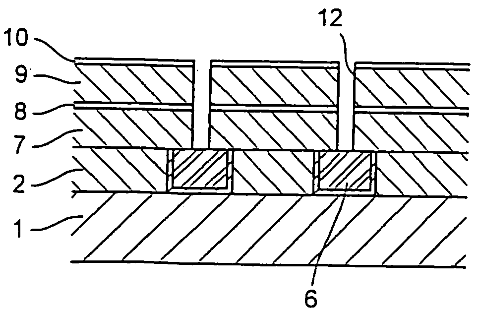
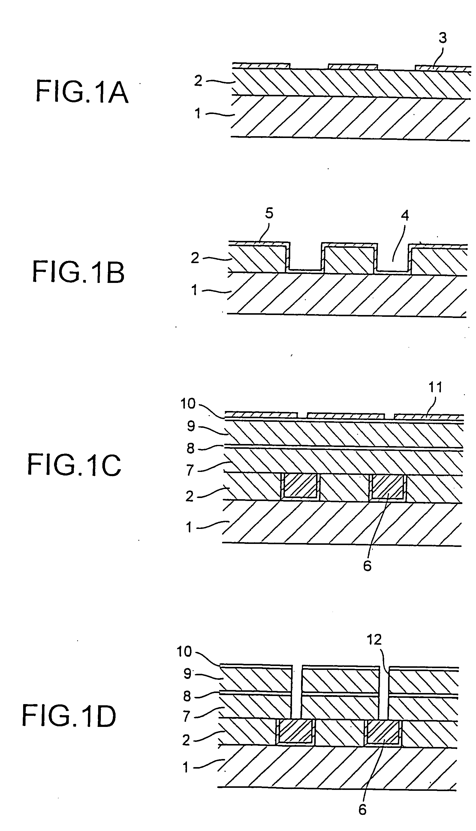
[0087] Four layers, i.e., an SiN layer, a first low dielectric material layer composed of a hydrogen silsesquioxane-based low dielectric material (trade name: OCD T-12 supplied from Tokyo Ohka Kogyo Co., Ltd.), an SiN layer and a second dielectric material layer composed of the hydrogen silsesquioxane-based low dielectric material (trade name: OCD T-12 supplied from Tokyo Ohka Kogyo Co., Ltd.) were sequentially laminated on a substrate on which a copper wiring had been formed to form an interlayer insulating layer of 6000 angstroms.

[0088] A first reflection preventing film with a film thickness of 770 angstroms composed of ARC-29 (supplied from Brewer Science) was formed on the above interlayer insulating layer, a first photoresist layer with a film thickness of 4000 angstroms was formed thereon, and exposure and development were given. The first photoresist layer was formed using a resist composition (trade name: TArF-7a21 supplied from Tokyo Ohka Kogyo Co., Ltd.) whose major ingr...

examples 2 to 5

[0096] Each dual damascene structure was formed in the same way as in Example 1 except that the first and second reflection preventing films in the Example 1 were constituted from the following four resin compositions.

[0097] As the reflection preventing film-forming materials, the following resin compositions of (A), (B), (C) and (D) were prepared.

[0098] (A) Resin composition where a resin component composed of ethyl p-styrenesulfonate was dissolved in a solvent composed of γ-butyrolactone / ethyl lactate (2:8) and a solid concentration was adjusted to 6% by weight.

[0099] (B) Resin composition where a resin component composed of ethyl p-styrenesulfonate:hydroxyethyl acrylate (=5:5) and Cymel 1172 (tetramethylol glycoluril supplied from Mitsui Cyanamid Co., Ltd.) at an amount equivalent to 20% by weight based on the resin component amount were dissolved in the solvent composed of ethyl lactate and the solid concentration was adjusted to 6% by weight.

[0100] (C) Resin composition whe...

example 6

[0104] A dual damascene structure was formed in the same way as in Example 1 except that the first and second reflection preventing films in Example 1 were constituted from the following resin composition.

[0105] Tetraisopropoxy titanium (100 g) was dissolved in 338 g of ethanol, and then 121 g of acetic acid and 357 g of acetyl acetone were added to obtain a mixture. This mixture was stirred for 4 hours and subsequently left stand for 16 hours to obtain a solution of 10% polytitanoxane.

[0106] Subsequently, 113 g of methanol, 312 g of acetyl acetone and 324 g of acetic acid were added to 324 g of tetraethoxysilane to obtain a mixture. This mixture was stirred for 6 hours and subsequently left stand for 16 hours to obtain a solution of 9% polysiloxane.

[0107] A resin mixed solution obtained by mixing the polytitanoxane solution and the polysiloxane solution at 1:1 and diluting with butyl cellosolve was a material for forming the first and second reflection preventing films correspon...


PUM


Abstract

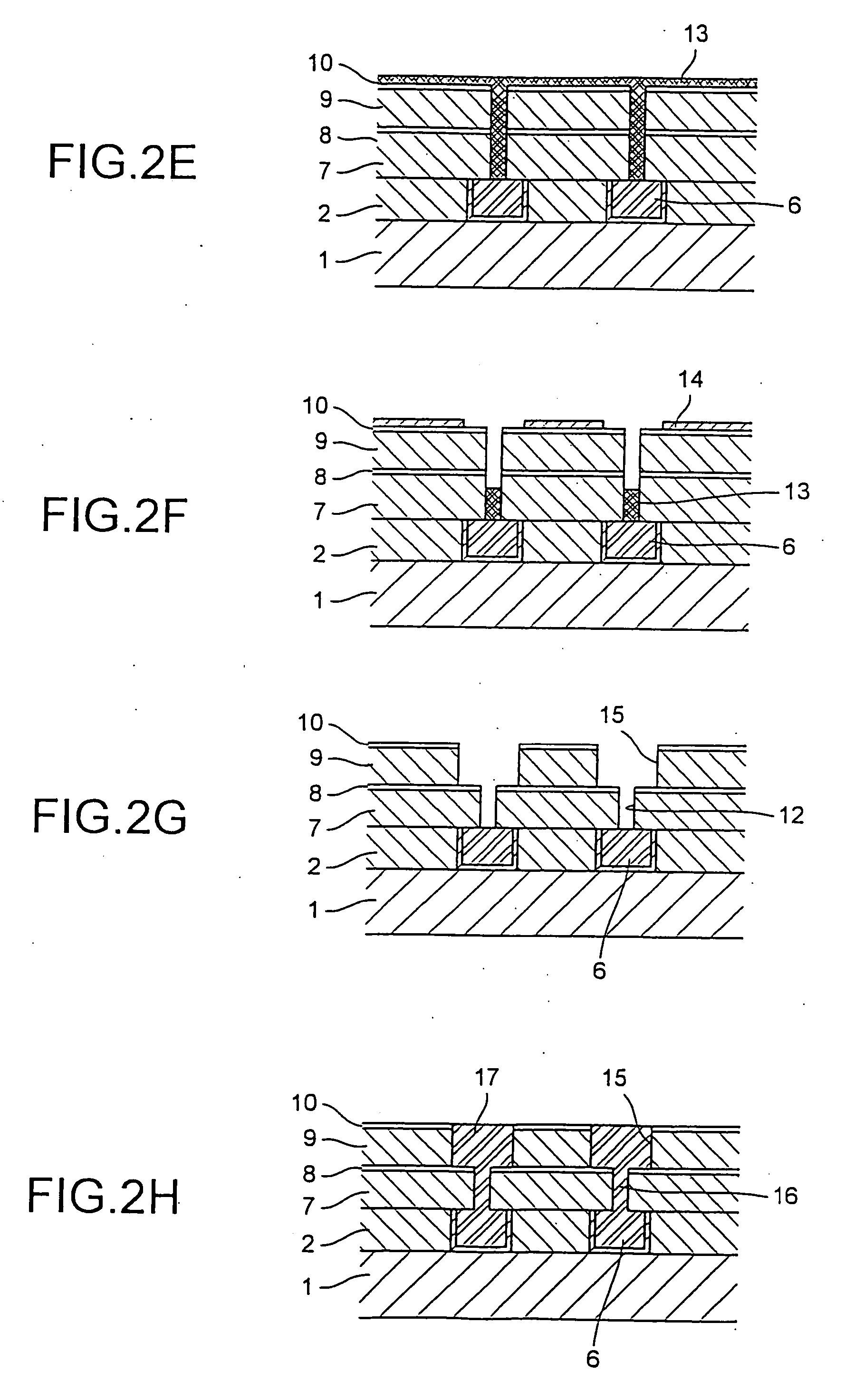
In a method for forming a wiring using a dual damascene process in which a multilayer wiring structure is formed by embedding a first etching space formed in an interlayer insulating layer and a second etching space which communicates thereto with a conductor material, a number of steps may be reduced and flexibility in the step management is enhanced without deteriorating a low dielectric material layer which constitutes the interlayer insulating layer. Therefor, a filler material whose major ingredient is a spin-on-glass material capable of being easily removed by a stripping solution which gives no damage to the interlayer insulating layer is used as a material filled in the first etching space in order to protect a lower wiring layer from exposure light to form a photoresist pattern for forming the second etching space. Furthermore, no light absorbing material for absorbing the exposure light is added to this filler material. Instead, a reflection preventing film capable of being processed by dry etching or a reflection preventing film which is soluble in a developer is formed on a filler material layer.

Description

TECHNICAL FIELD [0001] The present invention relates to a method for forming a semiconductor multilayer wiring where a lower wiring layer formed on a semiconductor substrate and an upper wiring layer formed thereon by the intermediary of an interlayer insulating layer, in which the lower and the upper wiring layer are connected by a via wiring which penetrates the interlayer insulating layer, and more particularly relates to a method for forming a semiconductor multilayer wiring where the via wiring and the upper wiring layer are formed by a simpler dual damascene process. BACKGROUND ART [0002] As is well-known, in a basic wiring structure in a semiconductor integrated circuit, a lower wiring layer directly or indirectly formed on a semiconductor substrate and an upper wiring layer formed on this lower wiring layer by the intermediary of an interlayer insulating layer are connected by a via wiring formed to penetrate the interlayer insulating layer. A multilayer wiring structure in ...

Claims


Application Information

Patent Timeline
Patent Type & Authority Applications(United States)
IPC IPC(8): H01L21/8238H01L21/3205H01L21/3213H01L21/768
CPCH01L21/76808H01L21/76807
Inventor HAGIWARA, YOSHIOTANAKA, TAKESHI
Owner TOKYO OHKA KOGYO CO LTD
Learn More