Semiconductor device and method for fabricating the same

a technology of semiconductors and semiconductors, applied in the direction of solid-state devices, transistors, electric devices, etc., can solve the problems of increased defect generation, increased electrode layer, and increased risk of damage to the upper electrode layer, and achieve the effect of improving device characteristics and simplifying the fabrication process

Inactive Publication Date: 2006-07-06
ATRIA TECH INC
View PDF10 Cites 29 Cited by
  • Summary
  • Abstract
  • Description
  • Claims
  • Application Information

AI Technical Summary

Benefits of technology

[0024] It is, therefore, an object of the present invention to provide a semiconductor device and a method for fabricating the same, wherein the semiconductor device is obtained by a simplified fabrication process, which forms a MIM type capacitor and then a metal interconnection line, and has an improved device characteristic.

Problems solved by technology

However, it is often complicated to form the MIM type capacitors in the Cu Back-end-of-Line (BEOL), thereby increasing a defect generation.
However, the etching of the upper electrode layer 50 may damage those first metal interconnection lines 20 exposed by the above etching process for forming the MIM type capacitor structure.
The defects may become a cause for decreasing reliability of semiconductor devices.
However, the additional use of the photoresist mask makes the capacitor fabrication process complicated, and it is difficult to fabricate such photoresist mask that masks only the first metal interconnection lines 20.
However, it is required to form overlay keys or alignment keys additionally, thereby resulting in a complicated fabrication process.
Hence, a defect generation is more likely to occur.

Method used


Image

  • Semiconductor device and method for fabricating the same
  • Semiconductor device and method for fabricating the same
  • Semiconductor device and method for fabricating the same

Examples


Embodiment Construction

[0031] A semiconductor device and a method for fabricating the same in accordance with exemplary embodiments of the present invention will be described in detail with reference to the accompanying drawings.

[0032]FIGS. 3A to 3F are cross-sectional views of a semiconductor device fabricated in accordance with a specific embodiment of the present invention for illustrating a fabrication method thereof.

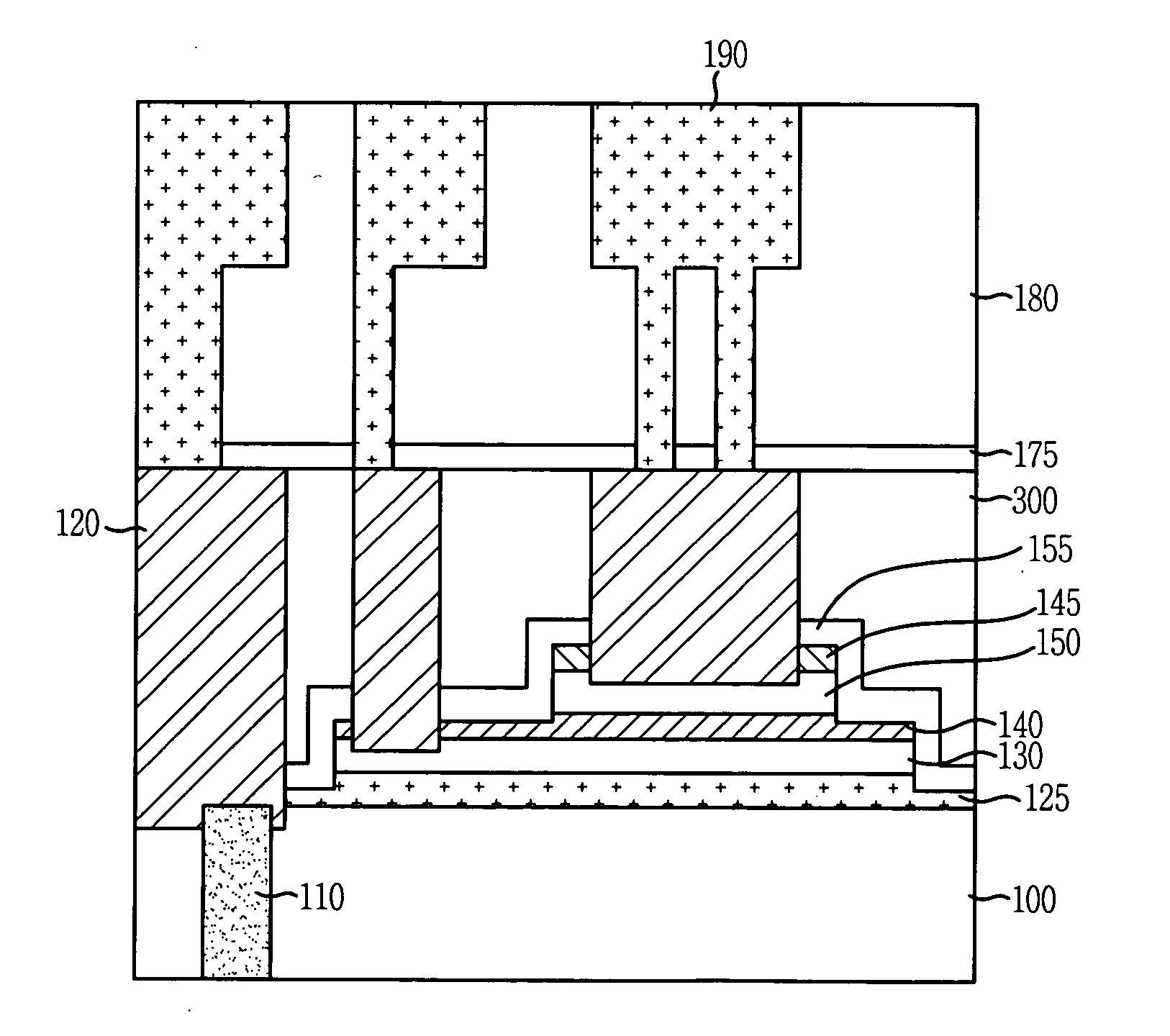
[0033] Referring to FIG. 3A, a contact plug 110 is formed within an inter-layer insulation layer 100, and a first nitride-based layer 125, a lower electrode layer 130, a dielectric layer 140, an upper electrode layer 150, and a second nitride-based layer 145 are sequentially formed on the contact plug 110 and on the inter-layer insulation layer 100. The lower electrode layer 130 and the upper electrode layer 150 include a material selected from the group consisting of titanium nitride (TiN), tantalum nitride (TaN), aluminum (Al), tungsten (W), and copper (Cu). The dielectric layer 140 i...


PUM

PropertyMeasurementUnit
series resistanceaaaaaaaaaa
capacitanceaaaaaaaaaa
thermal stabilityaaaaaaaaaa

Abstract

A semiconductor device and a method for fabricating the same are provided. The method includes: forming a contact plug passing through an inter-layer insulation layer; sequentially forming a lower electrode layer, a dielectric layer and an upper electrode layer on the inter-layer insulation layer; patterning the upper electrode layer; patterning the dielectric layer and the lower electrode layer, thereby obtaining a capacitor including an upper electrode, a patterned dielectric layer and a lower electrode; and sequentially forming a first metal interconnection line connected with the contact plug and second metal interconnection lines connected with the capacitor.

Description

FIELD OF THE INVENTION [0001] The present invention relates to a semiconductor device and a method for fabricating the same; and, more particularly, to a semiconductor device and a method for fabricating the same, wherein the semiconductor device includes a metal-insulator-metal capacitor formed before a metal interconnection line is formed. DESCRIPTION OF RELATED ARTS [0002] Analog capacitors applied to integrated circuit (IC) logic devices of complementary metal oxide semiconductor (CMOS) image sensors generally require high accuracy. Such semiconductor technology is essential in technical fields related to analog-to-digital (AD) converters and switched capacitor filters. [0003] There have been various capacitor structures including a structure of polysilicon to polysilicon, a structure of polysilicon to silicon, a structure of metal to silicon, a structure of metal to polysilicon, a structure of metal to metal, and a structure of metal-insulation-metal (MIM). Among these capacito...

Claims


Application Information

Patent Timeline
Patent Type & Authority Applications(United States)
IPC IPC(8): H01L29/00
CPCH01L23/5223H01L28/40H01L2924/0002H01L2924/00H01L21/76897H01L21/31144H01L21/02041H01L28/75
Inventor CHO, JIN-YOUN
Owner ATRIA TECH INC
Why Eureka
Try Eureka