Method of manufacturing micro structure, and method of manufacturing mold material

Inactive Publication Date: 2006-07-06
SONY CORP
View PDF8 Cites 18 Cited by
  • Summary
  • Abstract
  • Description
  • Claims
  • Application Information

AI Technical Summary

Benefits of technology

[0017] The focused energy beam permits easy control over the diameter and length of the pore and microstructure if the apparatus is run under adequate conditions.
[0018] Also, owing to its high positional resolut

Problems solved by technology

These materials, however, are hard to handle because of their small size.
However, the use of FIB disclosed in the past is nothing more than energy irradiation.
Making pores in alumina by anodic oxidation (which is a chemical process) presents difficulties with controlling

Method used


Image

  • Method of manufacturing micro structure, and method of manufacturing mold material
  • Method of manufacturing micro structure, and method of manufacturing mold material
  • Method of manufacturing micro structure, and method of manufacturing mold material

Examples


example 1

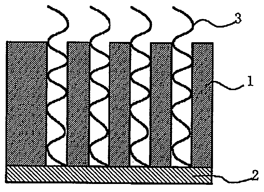
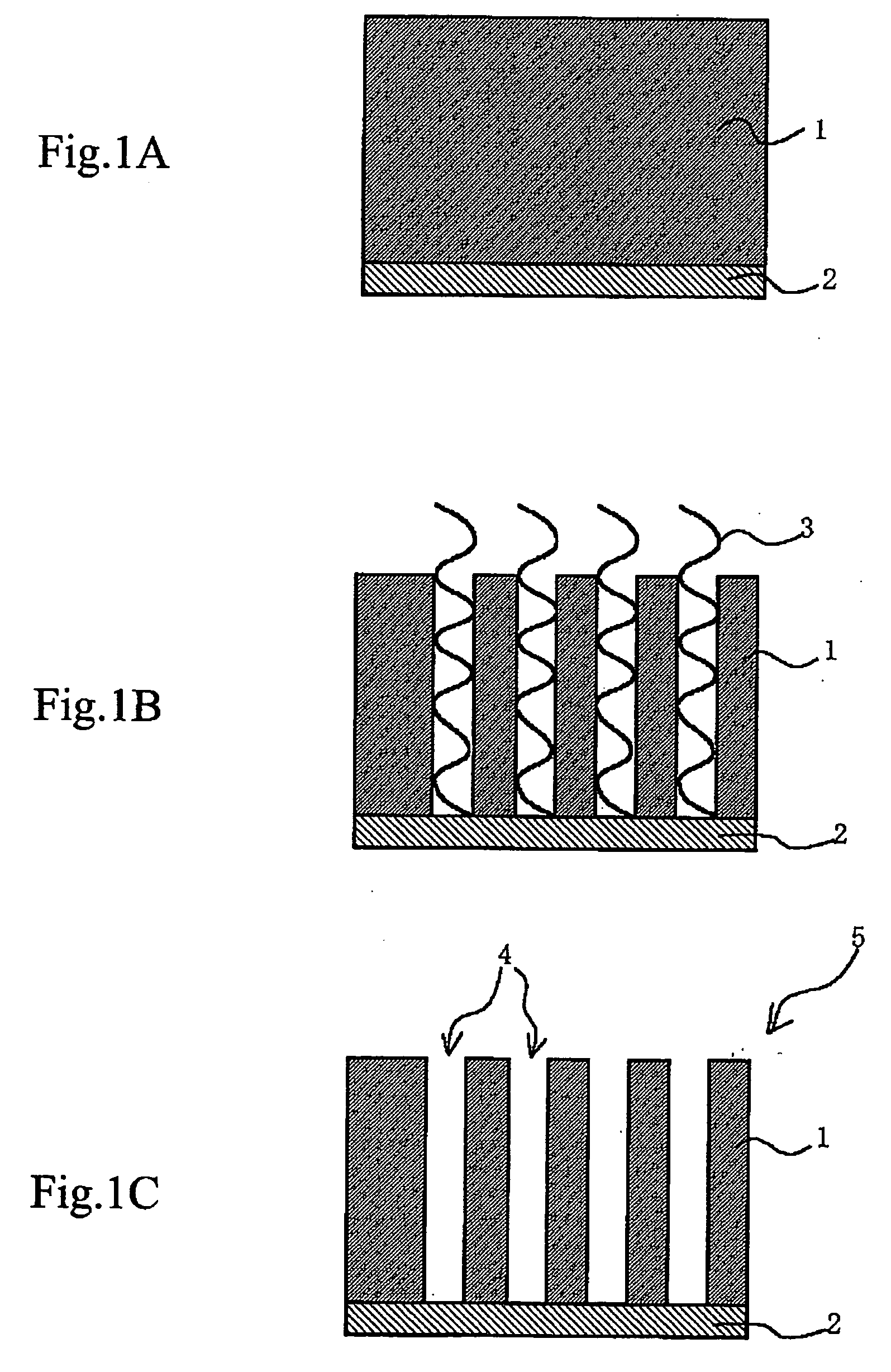
[0073] An aluminum substrate measuring 5 mm square was cut out of an aluminum sheet of high purity (99.999%). After degreasing with acetone and cleaning with ethanol, the aluminum substrate was fixed with a conductive paste and allowed to stand in a vacuum (approximately 10−5 Pa) for 30 minutes.

[0074] The aluminum substrate was irradiated with a Ga+ beam at an accelerating voltage of 30 kV and a beam current of 15 pA by using FB2000 (made by Hitachi). The beam was focused so that the beam diameter was 10 nm. It is to be noted that the Ga ion beam may be replaced by any other cation beam. The irradiating position of the ion beam was controlled within an error of ±5 nm by observing under an electron microscope. Irradiation with the ion beam was carried out to make pores, each measuring 10 nm in diameter and 2 μm in depth, at intervals of 20 nm, in the aluminum substrate. The rate of etching by irradiation was about 0.008 μm3 / s. The pore density was as high as 1.25×10¹¹ pores / cm2. Inc...

example 2

[0079] An aluminum substrate measuring 5 mm square was cut out of an aluminum sheet of high purity (99.999%). After degreasing with acetone and cleaning with ethanol, the aluminum substrate was fixed with a conductive paste and allowed to stand in a vacuum (approximately 10-5 Pa) for 30 minutes.

[0080] The aluminum substrate was irradiated with a Ga+ beam at an accelerating voltage of 30 kV and a beam current of 15 pA by using FB2000 (made by Hitachi). The beam was focused so that the beam diameter was 20 nm. It is to be noted that the Ga ion beam may be replaced by any other cation beam.

[0081] The irradiating position of the ion beam was controlled within an error of ±5 nm by observing under an electron microscope. Irradiation with the ion beam was carried out to make pores, each measuring 20 nm in diameter and 2 μm in depth, at intervals of 100 nm, in the aluminum substrate. The rate of etching by irradiation was about 0.008 μm3 / s. The pore density was as high as 1.25×10¹¹ pores / ...

example 3

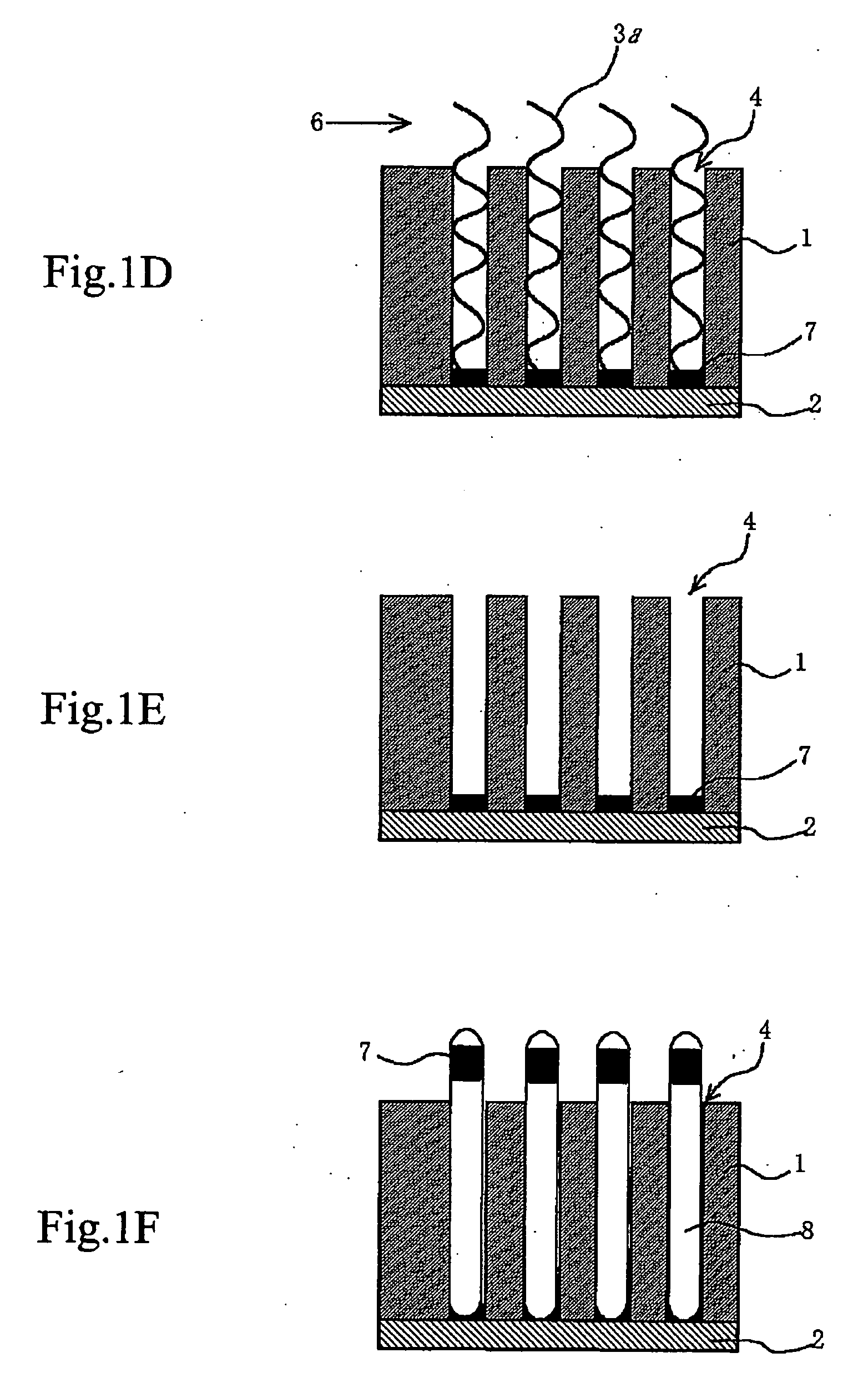
[0085] This example is intended to obtain the microstructure that would be applicable to the memory device.

[0086] First, an aluminum substrate measuring 5 mm square was cut out of an aluminum sheet of high purity (99.999%). After degreasing with acetone and cleaning with ethanol, the aluminum substrate was fixed with a conductive paste and allowed to stand in a vacuum (approximately 10−5 Pa) for 30 minutes.

[0087] Then, the aluminum substrate was irradiated with a Ga+ beam at an accelerating voltage of 30 kV and a beam current of 15 pA by using FB2000 (made by Hitachi). The beam was focused so that the beam diameter was 10 nm. It is to be noted that the Ga ion beam may be replaced by any other cation beam. The irradiating position of the ion beam was controlled within an error of ±5 nm by observing under an electron microscope. Irradiation with the ion beam was carried out to make pores, each measuring 10 nm in diameter and 2 μm in depth, at intervals of 20 nm, in the aluminum subs...


PUM

PropertyMeasurementUnit
Diameteraaaaaaaaaa
Nanoscale particle sizeaaaaaaaaaa

Abstract

Disclosed herein are a method of producing microstructure and a method of producing mold, the methods permitting production of much smaller pores than before in an atmosphere where impurities are negligible and also permitting production of microstructures having a smaller size and a higher crystallinity than before with the help of the pores. The method of producing microstructure comprises a step of making pores (4) in a substrate (1) to become a mold (5) by irradiation with a focused energy beam (3) and a step of growing a microstructure (8) in the thus made pores (4). The method of producing a mold includes a step of making pores (4) by irradiating a substrate (1) to become a mold (5) with a focused energy beam (3).

Description

TECHNICAL FIELD [0001] The present invention relates to a method of producing microstructure and a method of producing mold. BACKGROUND ART [0002] Because microfabrication by top-down approach is physically limited (by the wavelength of laser beam), one-dimensional nanoscale microstructures are expected to play an important role for electronic devices. Intensive research and development works are going on in this field. [0003] Among typical topics of such research are carbon nanotube (CNT) and metal nanowire. These materials, however, are hard to handle because of their small size. Their practical use will be feasible only after 2010 on account of problems with assembling and integration. [0004] Active researches are going on for the method of their synthesis with a high degree of orientation. The resulting materials are expected to find use in field emission display and memory. There has been proposed a method of producing CNT by vapor phase growth in pores in zeolite or anodized a...

Claims


Application Information

Patent Timeline
IPC IPC(8): H01J9/04H01J9/02H01J1/14H01J9/24H01J1/02B82B3/00B01J23/75B01J37/02B01J37/03B01J37/34C01B31/02C23C16/44C23C16/48
CPCB01J37/34B82Y10/00B82Y30/00B82Y40/00C01B31/0233C01B31/0293C30B25/18C30B29/02C30B29/602G11C2213/81H01J9/025Y10S977/842Y10S977/876Y10S977/893C01B32/162C01B32/18B82B3/00B01J37/02C23C16/44
Inventor KADONO, KOJIMURAKAMI, YOSUKE
Owner SONY CORP
Why Eureka
Try Eureka