Gallium nitride-based devices and manufacturing process

a technology of gallium nitride and manufacturing process, which is applied in the direction of crystal growth process, polycrystalline material growth, chemistry apparatus and processes, etc., to achieve the effect of reducing the electrical performance limitations of silicon substrates and achieving the resolution of electrical performance limitations

Inactive Publication Date: 2006-07-13
POWER INTEGRATIONS INC
View PDF32 Cites 37 Cited by
  • Summary
  • Abstract
  • Description
  • Claims
  • Application Information

AI Technical Summary

Benefits of technology

[0017] These aspects of the present invention incorporate the realization that the electrical performance limitations associated with a silicon substrate c...

Problems solved by technology

Further, it is believed that the superlattices tend to limit ...

Method used


Image

  • Gallium nitride-based devices and manufacturing process
  • Gallium nitride-based devices and manufacturing process
  • Gallium nitride-based devices and manufacturing process

Examples


Embodiment Construction

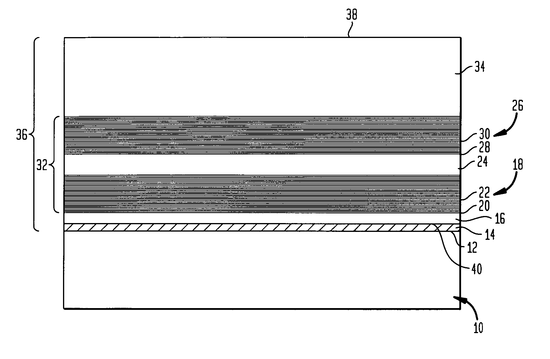
[0030] As used in the present disclosure, the term “III-V semiconductor” refers to a compound semiconductor material according to the stoichiometric formula AlaInbGacNdAsePf where (a+b+c) is about 1 and (d+e+f) is also about 1. The term “nitride semiconductor” or “nitride-based semiconductor” refers to a III-V semiconductor in which d is 0.5 or more, most typically about 0.8 or more. Most preferably, the semiconductor materials are pure nitride semiconductors, i.e., nitride semiconductors in which d is about 1.0. The term “gallium nitride based semiconductor” as used herein refers to a nitride semiconductor including gallium, and most preferably including gallium as the principal metal present, i.e., having c≧0.5 and most preferably ≧0.8. The semiconductors may have p-type or n-type conductivity, which may be imparted by conventional dopants and may also result from the inherent conductivity type of the particular semiconductor material. For example, gallium nitride-based semiconduc...


PUM


Abstract

A nitride semiconductor is grown on a silicon substrate by depositing a few mono-layers of aluminum to protect the silicon substrate from ammonia used during the growth process, and then forming a nucleation layer from aluminum nitride and a buffer structure including multiple superlattices of AlRGa(1-R)N semiconductors having different compositions and an intermediate layer of GaN or other Ga-rich nitride semiconductor. The resulting structure has superior crystal quality. The silicon substrate used in epitaxial growth is removed before completion of the device so as to provide superior electrical properties in devices such as high-electron mobility transistors.

Description

CROSS-REFERENCE TO RELATED APPLICATIONS [0001] This application is a divisional of U.S. application Ser. No. 10 / 721,488, filed Nov. 25, 2003, and claims the benefit of U.S. Provisional Patent Application Ser. No. 60 / 430,837, filed Dec. 4, 2002, the disclosures of which are incorporated by reference herein.BACKGROUND OF THE INVENTION [0002] The present invention relates to nitride semiconductor structures and devices and to processes for making the same. [0003] Nitride semiconductors such as gallium nitride and related semiconductors are widely regarded as desirable wide bandgap compound semiconductors. These materials have been adopted in optoelectronic devices such as light-emitting diodes (“LEDs”), laser diodes and photodiodes, and have also been employed in non-optical electronic devices such as field effect transistors (“FETs”) and field emitters. In optoelectronic devices, the wide bandgap of the material allows for emission or absorption of light in the visible-to-ultraviolet ...

Claims


Application Information

Patent Timeline
IPC IPC(8): H01L21/20H01L21/36H01L31/20C30B29/68H01L21/205H01L29/15H01L29/20H01L33/00
CPCC30B29/68H01L21/02381H01L21/02458H01L21/02491H01L33/007H01L21/0254H01L29/155H01L29/2003H01L21/02507H01L21/20
Inventor GUO, SHIPINGGOTTHOLD, DAVIDPOPHRISTIC, MILANPERES, BORISELIASHEVICH, IVANSHELTON, BRYAN S.CERUZZI, ALEX D.MURPHY, MICHAELSTALL, RICHARD A.
Owner POWER INTEGRATIONS INC
Why Eureka
Try Eureka