Direct collection transmission electron microscopy

Inactive Publication Date: 2006-08-03
RGT UNIV OF CALIFORNIA
View PDF2 Cites 41 Cited by
  • Summary
  • Abstract
  • Description
  • Claims
  • Application Information

AI Technical Summary

Benefits of technology

[0010] In the invention, transmission electron microscopy is conducted with direct detection. An active pixel detector detects the incident signal,

Problems solved by technology

Existing detection techniques have drawbacks.
The main drawback, however, is the low resolution of the structures obtainable with conventional technology.
The first is difficulties with specimen stabilization and radiation damage.
The second are difficulties with the collection and processing of the very large data sets required for statistical analysis.
The use of film to record images is problematic.
While film provides excellent modulation transfer functions, especially in comparison with commercial CCD cameras, it requires several post-acquisition steps, including development and digitization, that are cumbersome and time-consuming.
Even prior to the post acquisition, the use of film is cumbersome.
The loading and unloading of film into a typical transmission electron microscope is a time-consuming procedure, and if the particular procedures are not followed

Method used


Image

  • Direct collection transmission electron microscopy
  • Direct collection transmission electron microscopy
  • Direct collection transmission electron microscopy

Examples


Embodiment Construction

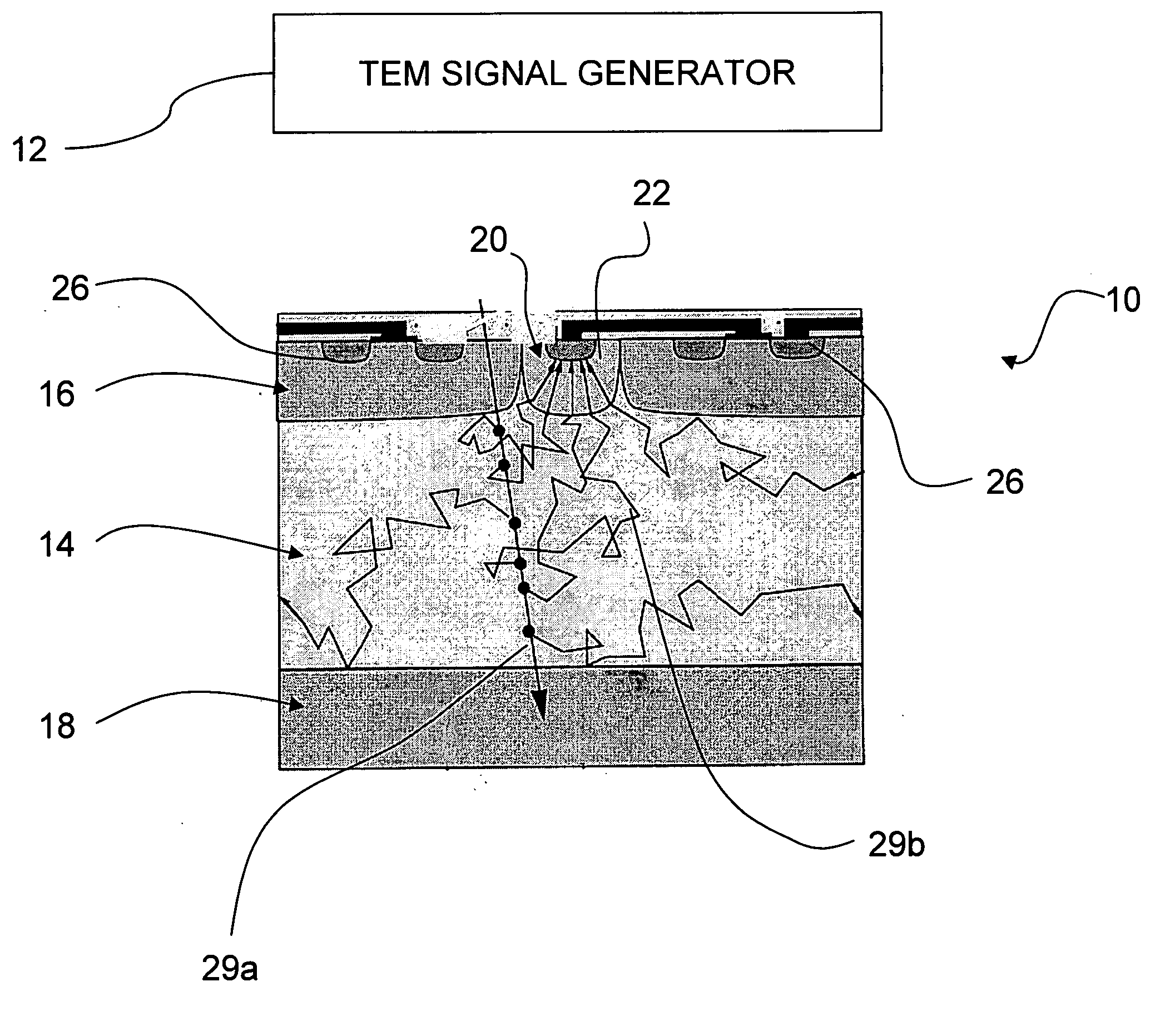
[0021] Embodiments of the invention provide a detector for transmission electron microscopy. Direct detection is achieved without film or a scintillation screen. A preferred embodiment active pixel detector of the invention has a plurality of pixels. Each pixel includes one or more photodiodes formed by a p-n junction to collect electrons generated by an incident high energy electron in its passage through an epitaxial layer into which the p-n junction is formed. Each pixel integrates the collected electrons during an exposure period. At the conclusion of the exposure period, the contents of the active pixel detector array can be read out, digitized and stored. In preferred embodiments, integration and read out electronics are implemented near the top surface of a chip, and are transparent to the incident electrons.

[0022] In a preferred embodiment, the epitaxial layer is formed on a substrate that is thin enough to limit or eliminate signals caused by backscattering of electrons fr...


PUM


Abstract

A preferred method for transmission electron microscopy includes a step of generating a microscopy signal. The microscopy signal is then detected with an active pixel detector that includes a plurality of pixels. Each of the pixels includes at least one photodiode. Each pixel integrates an incident signal over a collection time period. Using a massibel parallel on chip analog to digital conversion, very fast read out times can be achieved, e.g., many frames per second. In a preferred embodiment, the read out time permits there to be a single electron event recorded per pixel, indicating either a single electron or the lack thereof. This permits simple accumulation of the pixel counts for each pixel in read-out and storage electronics.

Description

PRIORITY CLAIM AND REFERENCE TO RELATED APPLICATION [0001] This application is related to and claims priority under 35 U.S.C. §119 from prior provisional application 60 / 634,408, which was filed on Dec. 8, 2004.FIELD OF THE INVENTION [0002] A field of the invention is transmission electron microscopy. BACKGROUND [0003] Transmission electron microscopy conducted conventionally involves the use of film, video cameras or CCD (charge coupled device) detectors to detect high energy charged particles directly or indirectly through the agency of a intervening electron-sensitive scintillator screen which allows information to be collected on photon sensitive devices. Existing detection techniques have drawbacks. [0004] Transmission electron microscopy has many applications. One important application is to the analysis of proteinstructure. Protein crystallography is the premier method to determine the 3D structures of large proteins, DNA or RNA / protein complexes, and viruses. [0005] Cryo-Elec...

Claims


Application Information

Patent Timeline
IPC IPC(8): G21K7/00
CPCH01J37/224H01J37/244H01J37/26H01J2237/2441H01J2237/24455
Inventor NGUYEN-HUU, XUONGELLISMAN, MARK H.KLEINFELDER, STUART
Owner RGT UNIV OF CALIFORNIA
Why Eureka
Try Eureka