Electrically conductive diamond electrodes
a diamond electrode and electrode technology, applied in the manufacture of electrode systems, cold cathode manufacturing, electric discharge tube/lamp manufacture, etc., can solve the problems of increased ohmic resistance, loss of electrocatalyst activity, and degradation of the electrocatalyst support, and achieve the effect of extreme dimensional stability of the diamond host/support and stable operation
- Summary
- Abstract
- Description
- Claims
- Application Information
AI Technical Summary
Problems solved by technology
Method used
Image
Examples
example 1
Experimental
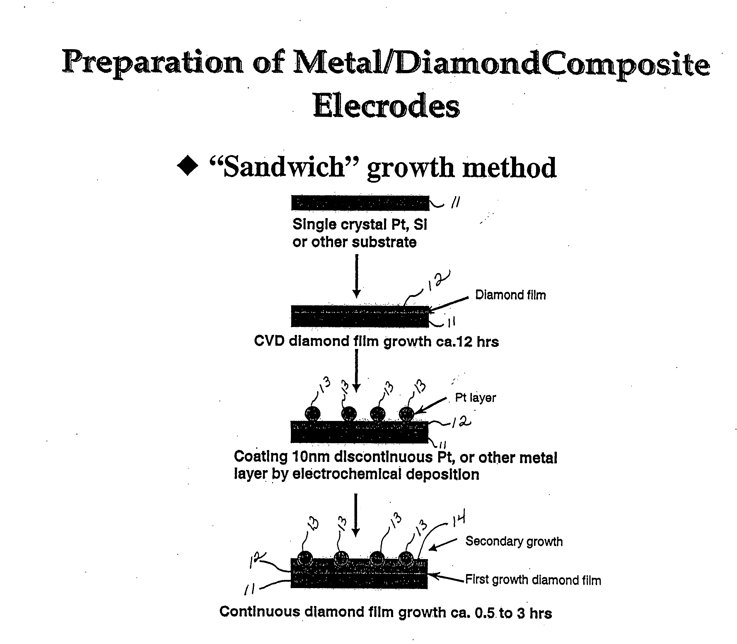
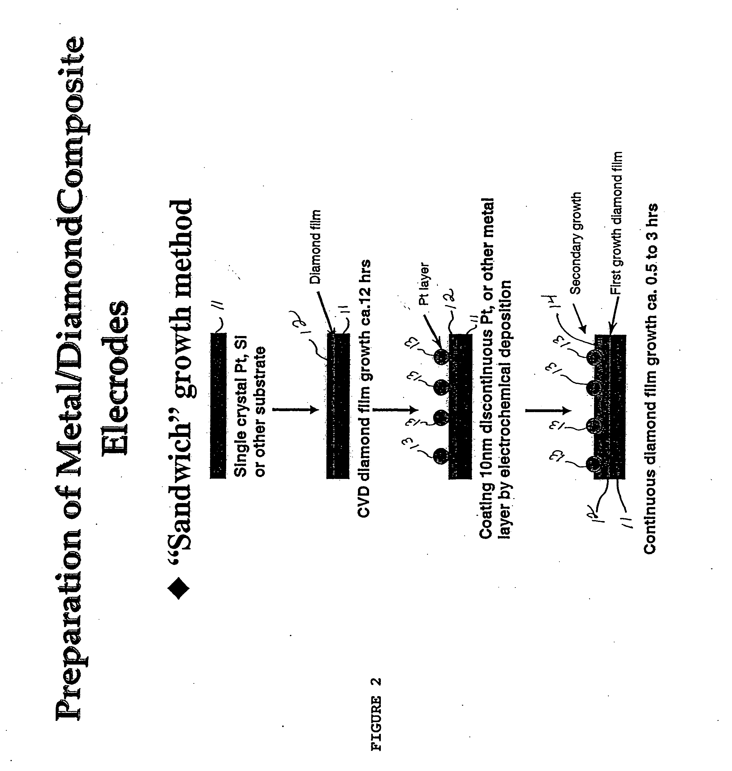
[0078] The boron-doped diamond thin films were deposited on p-Si (100) substrates (J. New Mater. Electrochem. Syst., 3 75 (2000); and Wang, J., et al., Electrochem. Solid-state Lett., 3 286 (2000)). The composite electrodes were prepared by initially depositing a ca. 3 μm thick boron-doped film for 12 h using a CH4 / H2 volumetric ratio of 0.35%. The microwave power was 1000 W, the pressure was ca. 40 to 60 Torr and the substrate temperature was ca. 875° C. The diamond growth was then stopped and the substrates cooled to less than 300° C. in the presence of atomic hydrogen. After cooling to room temperature, the film-coated substrates were removed from the reactor and a discontinuous layer of Pt particles was electrodeposited. The metal was electrodeposited from 1 mM K2PtCl6+0.1 M HClO4 using a constant current of 100 μA (500 μA / cm2) and a variable deposition time from 100 to 500 s. The Pt-coated films were then placed back in the CVD reactor and boron-doped diamond was ...
example 2
[0092] The preparation and characterization of an electrically conducting diamond powder formed by coating insulating diamond powder with a boron-doped diamond overlayer. Conductive powders were prepared using deposition times from 1 to 6 h. The surface area of this powder (˜2 m2 / g) is lower than that desired for an ideal support but, nevertheless, is a useful starting point for making a conductive powder and evaluating its physical, electrical, and electrochemical properties. The powder morphology and microstructure were characterized before and after conductive diamond growth by scanning electron microscopy (SEM) and Raman spectroscopy. X-ray diffraction (XRD) analysis was used to verify the crystallinity of the coated powder. Bulk electrical measurements were performed to determine the ohmic resistance of the packed powder (no binder) Electrodes for electrochemical testing were prepared by mixing the conductive powder with a polytetrafluoroethylene (PTFE) binder, casting a thin l...
PUM
| Property | Measurement | Unit |
|---|---|---|
| diameter | aaaaa | aaaaa |
| anodic current density | aaaaa | aaaaa |
| temperature | aaaaa | aaaaa |
Abstract
Description
Claims
Application Information


