Electrolytic copper plating bath and plating process therewith

Active Publication Date: 2006-09-21
C UYEMURA & CO LTD
View PDF2 Cites 28 Cited by
  • Summary
  • Abstract
  • Description
  • Claims
  • Application Information

AI Technical Summary

Benefits of technology

[0013] The present invention provides excellent filling properties for filling up a blind via-hole having a small diameter and a high aspect ratio, whereby the blind via-holes can be filled up without generati

Problems solved by technology

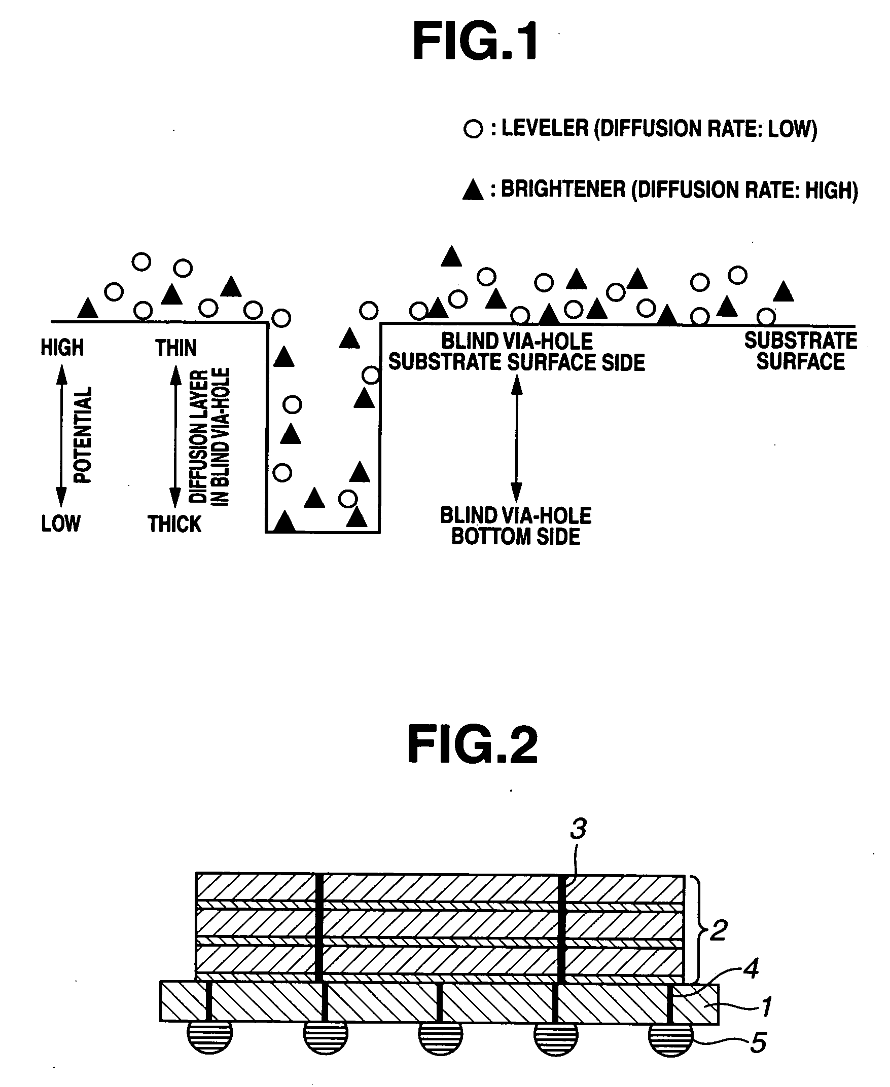
Therefore, where there is no effect of additive, deposition near the surface is more vigorous than deposition in the bottom portion, so that a cavity is generated, and the blind via-holes cannot be filled up with the copper plating film.
On the other hand, the supply of the leveler cannot catch up with the supply of the brightener on the blind via-hole bottom side where the diffusion layer is thicker, so that the plating-accelerating effect predominates there.
However, in the case of filling up a blind via-hole having a high aspect ratio, the use of a leveler (e.g., Janus green or the like) effective for via-filling plating in the cases of blind via-holes h

Method used


Image

  • Electrolytic copper plating bath and plating process therewith
  • Electrolytic copper plating bath and plating process therewith
  • Electrolytic copper plating bath and plating process therewith

Examples


example 1

[0062] A silicon wafer was provided with blind via-holes having an aperture portion of 50 μm square, a depth of 150 μm and an aspect ratio of 3.0 by etching, and an insulation layer was formed on the inside walls of the blind via-holes. Then, a Cu diffusion barrier layer (TiN) as a plating base coat layer and a seed layer (Cu) for the start of plating were formed on the wafer. The wafer was plated for via-filling by use of an electrolytic copper plating bath containing 200 g / L of copper sulfate pentahydrate, 50 g / L of sulfuric acid, 50 mg / L of chloride ions, 2 mg / L of SPS [bis-(3-sodiumsulfopropyl) disulfide] as a brightener, 500 mg / L of PEG [polyethylene glycol (average molecular weight: 7500)] as a carrier, and 5 mg / L of a copolymer of vinylpyrrolidone (VP) and vinylimidazolium chloride (VICl) (average molecular weight: about 60000 (corresponding to p=20 and q=400 in the above formula (2)); VP:VICl=5:95 (mol ratio)) as a leveler, under the conditions of CD=0.5 A / dm2 and a plating ...

example 2

[0064] A silicon wafer was provided with blind via-holes having an aperture portion of 50 μm square, a depth of 150 μm and an aspect ratio of 3.0 by etching, and an insulation layer was formed on the inside walls of the blind via-holes. Thereafter, a Cu diffusion barrier layer (TiN) as a plating base coat layer and a seed layer (Cu) for the start of plating were formed on the wafer. The wafer was plated for via-filling by use of an electrolytic copper plating bath containing 50 g / L of copper sulfate pentahydrate, 100 g / L of sulfuric acid, 70 mg / L of chloride ions, 15 mg / L of DDPS [sodium N,N-dimethyl-dithiocarbamylpropylsulfonate] as a brightener, 50 mg / L of PEG [polyethylene glycol (average molecular weight: 7500)] as a carrier, and 5 mg / L of a copolymer of vinylpyrolidone (VP) and vinylimidazolium chloride (VICl) (average molecular weight: 60000 (corresponding to p=20 and q=400 in the above formula (2)); VP:VICl=5:95 (mol ratio)) as a leveler, under the conditions of CD=0.5 A / dm2 ...

example 3

[0066] A silicon wafer was provided with blind via-holes having an aperture portion of 50 μm square, a depth of 150 μm and an aspect ratio of 3.0 by etching, and an insulation layer is formed on the inside walls of the blind via-holes. Thereafter, a Cu diffusion barrier layer (TiN) as a plating base coat layer and a seed layer (Cu) for the start of plating were formed on the wafer. The wafer was plated for via-filling by use of an electrolytic copper plating bath containing 250 g / L of copper sulfate pentahydrate, 40 g / L of sulfuric acid, 150 mg / L of chloride ions, 0.1 mg / L of OES [O-ethyl-S-(3-propylsulfonic acid-1)dithiocarbonate potassium salt] as a brightener, 200 mg / L of PO-EO [ethylene glycol-propylene glycol copolymer (average molecular weight: 1500)] as a carrier, and 5 mg / L of PVICl [polyvinylimidazolium chloride (average molecular weight: about 60000 (corresponding to m=400 in the above formula (1)))] as a leveler, under the conditions of CD=0.5 A / dm2 and a plating time of ...


PUM

PropertyMeasurementUnit
Diameteraaaaaaaaaa
Lengthaaaaaaaaaa
Lengthaaaaaaaaaa

Abstract

An electrolytic copper plating bath used for via-filling plating of blind via-holes formed on a substrate, containing a water-soluble copper salt, sulfuric acid, chloride ions, and a leveler as an additive, wherein the leveler is either one or both of a quaternary polyvinylimidazolium compound represented by the following formula (1) and a copolymer, represented by the following formula (2), of vinylpyrrolidone and a quaternary vinylimidazolium compound:
where R1 and R2 are each an alkyl group, m is an integer of not less than 2, and p and q are each an integer of not less than 1, and a copper electroplating method for via-filling plating of blind via-holes formed on a substrate by use of the electrolytic copper plating bath.

Description

BACKGROUND OF THE INVENTION [0001] The present invention relates to an electrolytic copper plating bath and a plating process therewith which show excellent filling properties in plating of a substrate having blind via-holes with small diameter and high aspect ratio and which are suitable also for performing via-filling plating and through-hole plating simultaneously for a substrate having both blind via-holes and through-holes. [0002] With the progress of reduction in size of electronic component parts and attendant on the demand for enhanced degrees of integration, the packaging has also been shifting from the peripheral terminal mounting and area terminal mounting toward the three-dimensional mounting. Therefore, in relation to semiconductor chips and interposers, researches of conduction or junction by through-electrodes have been under toward practical use thereof. In the case of the through-electrodes, like in the cases of via-filling for printed circuit boards and copper Dama...

Claims


Application Information

Patent Timeline
IPC IPC(8): C25D3/38
CPCC25D3/38H05K3/423
Inventor ISONO, TOSHIHISATACHIBANA, SHINJIKAWASE, TOMOHIROOMURA, NAOYUKI
Owner C UYEMURA & CO LTD
Why Eureka
Try Eureka