Silicon-on-nothing metal oxide semiconductor field effect transistor and method of manufacturing the same

a technology of metal oxide and semiconductors, applied in the direction of semiconductor devices, electrical equipment, basic electric elements, etc., can solve the problems of high leakage current flow between the source and drain, deterioration of device characteristics, and inability to meet the requirements of the application

Inactive Publication Date: 2006-09-21
KOREA ADVANCED INST OF SCI & TECH
View PDF0 Cites 28 Cited by
  • Summary
  • Abstract
  • Description
  • Claims
  • Application Information

AI Technical Summary

Benefits of technology

[0019] It is an object of the present invention to provide a SON MOSFET in which blisters are formed within a silicon substrate, so that a threshold voltage can be controlled by applying a voltage to the silicon substrate as in the bulk structure and the floating body effect and the self-heating effect, which are the biggest problems of the SOI structure, can be prohibited.

Problems solved by technology

Several problems that deteriorate device characteristics arise along with the continuous high integration of the semiconductor devices.
For this reason, there arises a problem, such as a short channel effect in which a high leakage current flows between the source and drain even when the transistor is turned off.
The method is, however, disadvantageous in that a manufacturing process is too complicated and control of elements (devices) / process parameters is difficult.
However, a floating body effect in which control of the leakage current or a critical (threshold) voltage in the semiconductor device becomes very difficult due to variation in the leakage current or the critical (threshold) voltage since the electric potential of the junction region in which the silicon channel 11 is formed is floated, a self-heating effect, and so on are generated.
A process is also complicated.

Method used


Image

  • Silicon-on-nothing metal oxide semiconductor field effect transistor and method of manufacturing the same
  • Silicon-on-nothing metal oxide semiconductor field effect transistor and method of manufacturing the same
  • Silicon-on-nothing metal oxide semiconductor field effect transistor and method of manufacturing the same

Examples


Embodiment Construction

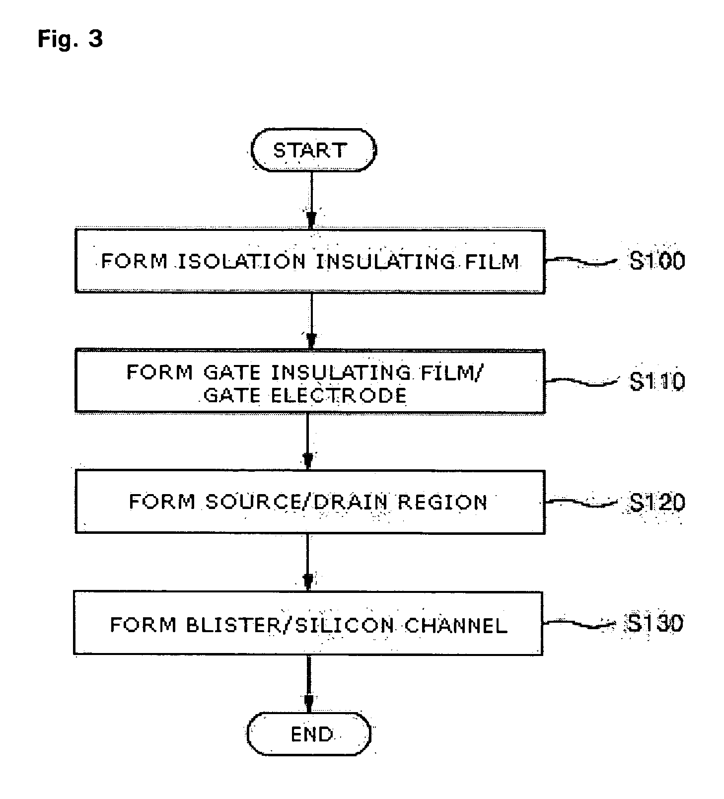
[0047] The present invention will now be described in connection with preferred embodiments with reference to the accompanying drawings.

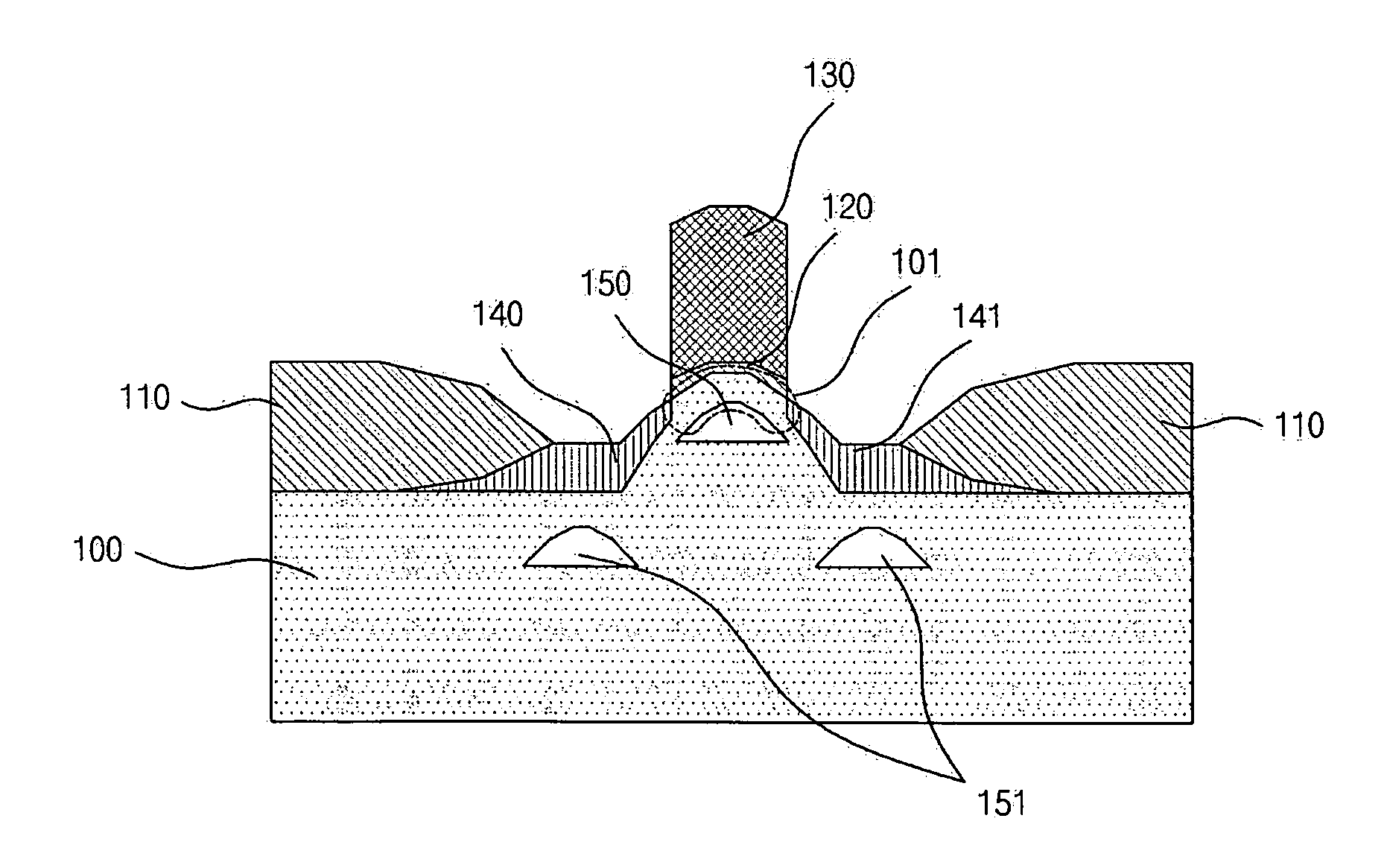
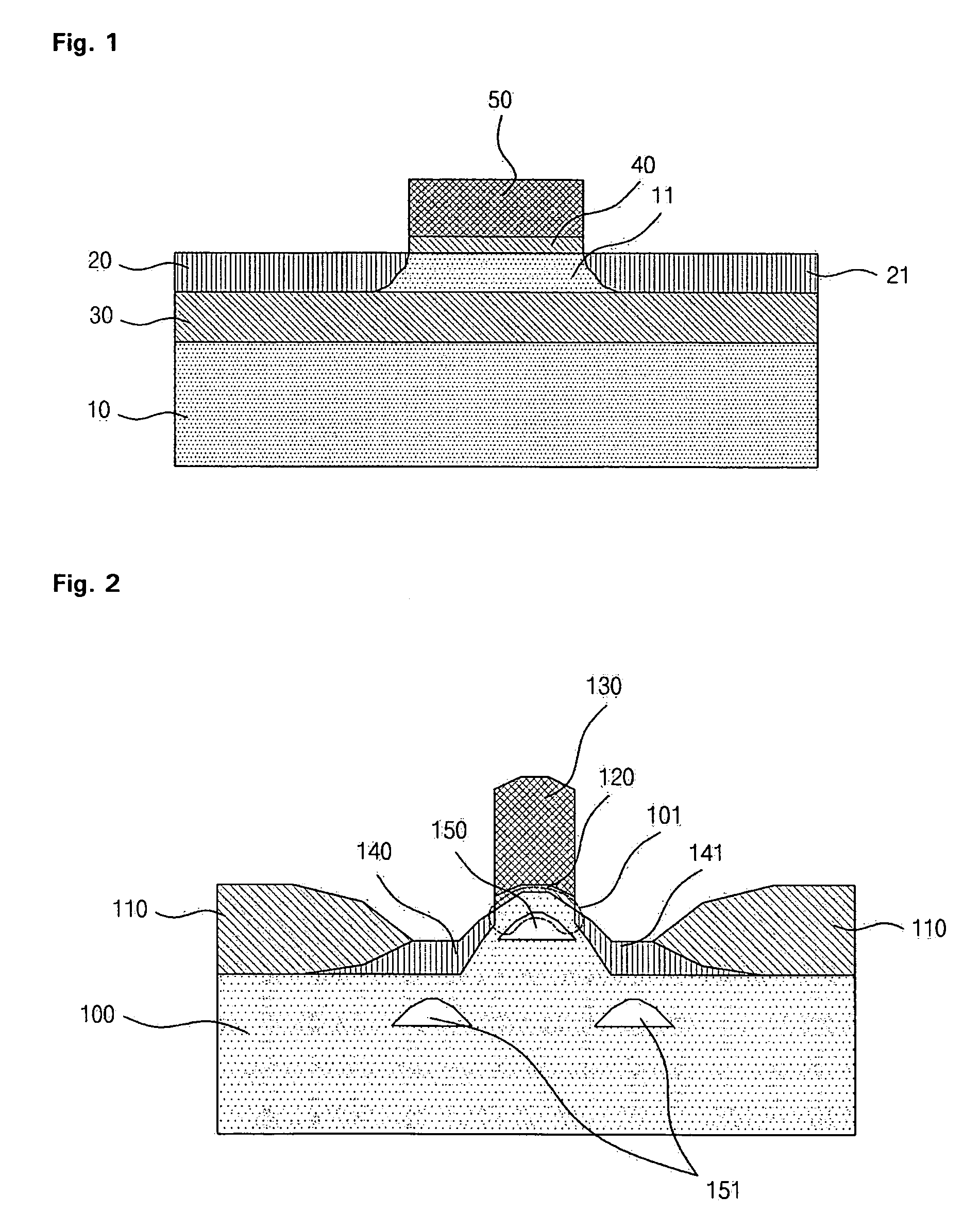
[0048] A SON MOSFET according to an embodiment of the present invention will be described below with reference to FIG. 2. FIG. 2 is a cross-sectional view of a SON MOSFET according to an embodiment of the present invention.

[0049] Referring to FIG. 2, the SON MOSFET according to an embodiment of the present invention comprises a silicon substrate 100, isolation insulating films 110, a gate insulating film 120, a gate electrode 130, a source region 140, a drain region 141, blister 150, 151 and a silicon channel 101.

[0050] The isolation insulating films 110 are formed at both upper sides of the silicon substrate 100. The gate insulating film 120 and the gate electrode 130 are sequentially stacked on a surface of the silicon substrate 100, which is located between the isolation insulating films 110. The isolation insulating films 110 function to elec...


PUM


Abstract

The present invention relates to a SON MOSFET and method of manufacturing the same, in which a blister is formed within a silicon substrate, thus improving the disadvantages of a bulk structure and a Silicon-On-Insulator (SOI) structure at the same time. The SON MOSFET according to the present invention comprises isolation insulating films formed at both upper sides of a silicon substrate, a gate insulating film and a gate electrode that are sequentially formed on a surface of the silicon substrate between the isolation insulating films, a source region and a drain region that are formed on the silicon substrate between the gate insulating film and the isolation insulating films, a blister formed within the silicon substrate under the gate insulating film, and a silicon channel, which is surrounded by the blister, the source region and the drain region, within the silicon substrate, wherein the blister is formed of hydrogen or helium ion.

Description

CROSS-REFERENCE TO RELATED APPLICATION [0001] This Nonprovisional application claims priority under 35 U.S.C. §119(a) on Patent Application No. 10-2005-0022425 filed in Korea on Mar. 17, 2005, the entire contents of which are hereby incorporated by reference. BACKGROUND [0002] 1. Field of the Invention [0003] The present invention relates to a Silicon-On-Nothing (SON) Metal Oxide Semiconductor Field Effect Transistor (MOSFET) and method of manufacturing the same, and more particularly, to a SON MOSFET and method of manufacturing the same, in which a blister is formed within a silicon substrate, thus improving the disadvantages of a bulk structure and a Silicon-On-Insulator (SOI) structure at the same time. [0004] 2. Discussion of Related Art [0005] To lower the price of semiconductor devices and enhance the performance thereof, the semiconductor devices have been integrated in accordance with Moore's Law while being continuously shrunken. Several problems that deteriorate device cha...

Claims


Application Information

Patent Timeline
Patent Type & Authority Applications(United States)
IPC IPC(8): H01L29/06
CPCH01L21/263H01L21/26506H01L29/0649H01L29/0653H01L29/1037H01L29/66545H01L29/78654H01L29/78696H01L21/18
Inventor CHOI, YANG-KYUJANG, DONG-YOON
Owner KOREA ADVANCED INST OF SCI & TECH
Why Eureka
Try Eureka