[0088] Advantageous effects obtained by the representative embodiment of the invention, disclosed under the present application, are briefly described as follows.
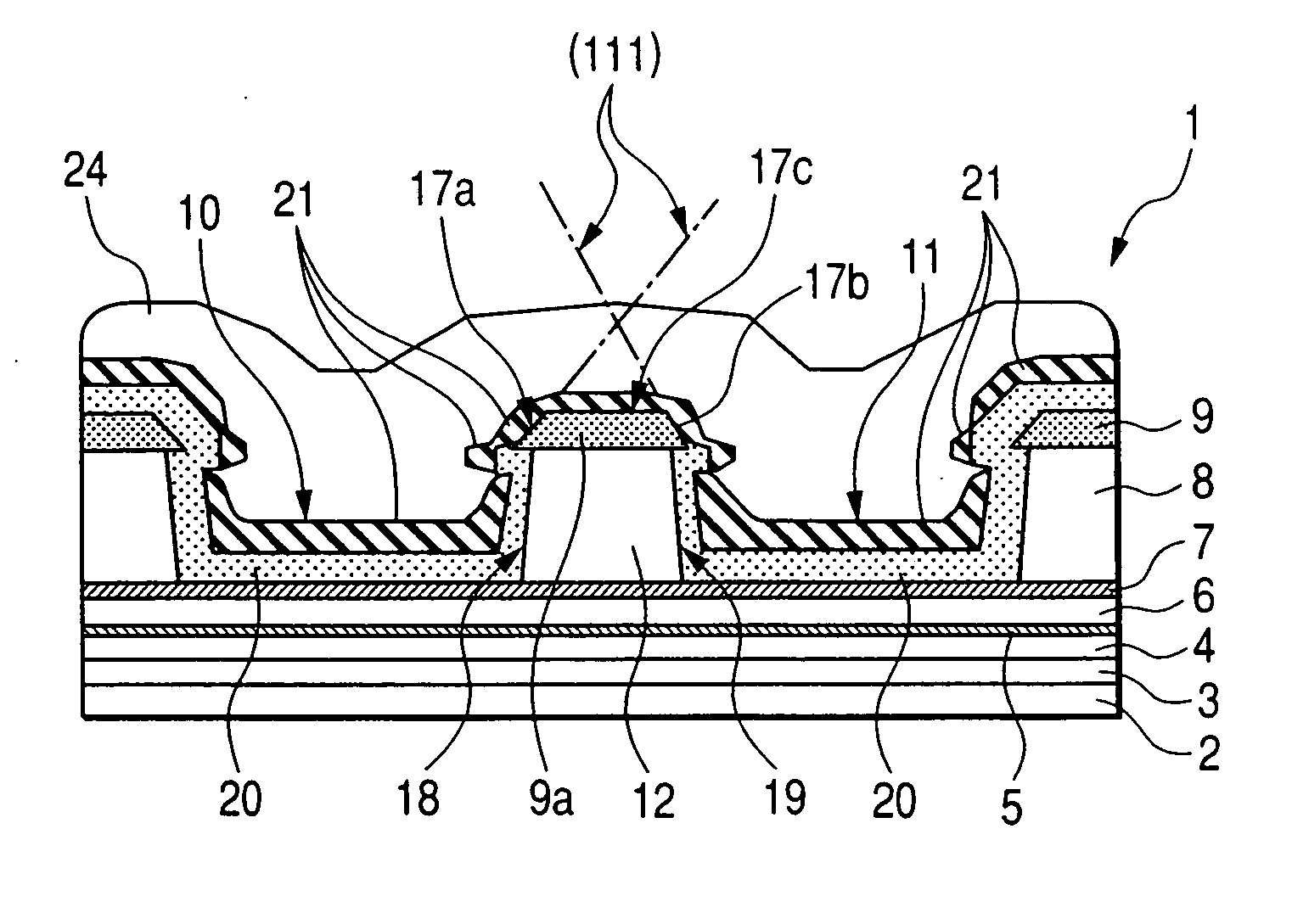
[0089] (a) According to means described under item (1) as above, the respective side faces of the ridge are covered with the insulating film, the respective side faces of the portion of the contact layer, corresponding to the ridge, constituting the upper part of the ridge, are the tilted faces, and obtuse angles are formed at corners of the top face of the portion of the contact layer, corresponding to the ridge, on the respective sides thereof, so that the portion of the contact layer, corresponding to the ridge, on the top face side thereof, can be reliably covered with the barrier metal layer.
[0090] (b) In the formation of the ridge, after forming the portion of the contact layer, corresponding to the ridge, and the portions of the contact layer, corresponding to the fields by
etching the contact layer, both side faces of the portion of the contact layer, corresponding to the ridge, are formed so as to become the tilted faces, respectively. Thereafter,
etching is applied twice, including the
dry etching and the wet etching each once, with the use of the portion of the contact layer, corresponding to the ridge, and the portions of the contact layer, corresponding to the fields, serving as the masks, to thereby form the separation grooves. As a result, a structure is formed such that the extremities of the portion of the contact layer, corresponding to the ridge, on the respective sides thereof, jut out toward the separation grooves, respectively; however, at least the undersides of the jutting out extremities of the portion of the contact layer, corresponding to the ridge, are covered with the insulating film. Further, the side faces of a portion of the second layer of the second cladding layer (the p-type cladding layer), forming a portion of the ridge, on the underside of the portion of the contact layer, corresponding to the ridge, are covered with portions of the insulating film 20, respectively, and the respective portions of the insulating film jut out further from the jutting out extremities of the portion of the contact layer, corresponding to the ridge, on the respective sides thereof, toward the respective separation grooves. As a result, a portion of the barrier metal layer 21 covering the portion of the contact layer, corresponding to the ridge, overlaps the portions of the insulating film 20 jutting out from the respective sides of the portion of the contact layer, corresponding to the ridge. Accordingly, the barrier metal layer and the insulating film, having such an advantageous effect as under (a) above, are linked with each other to thereby cover the portion of the contact layer, corresponding to the ridge, in such a way as to wrap the same up. Hence, the portion of the contact layer, corresponding to the ridge, is prevented from coming into contact with the first
electrode (p-
electrode) formed of Au, so that
diffusion of Au into the portion of the contact layer, corresponding to the ridge, can be deterred, and an optical
semiconductor device excellent in the characteristics thereof can be thereby manufactured.
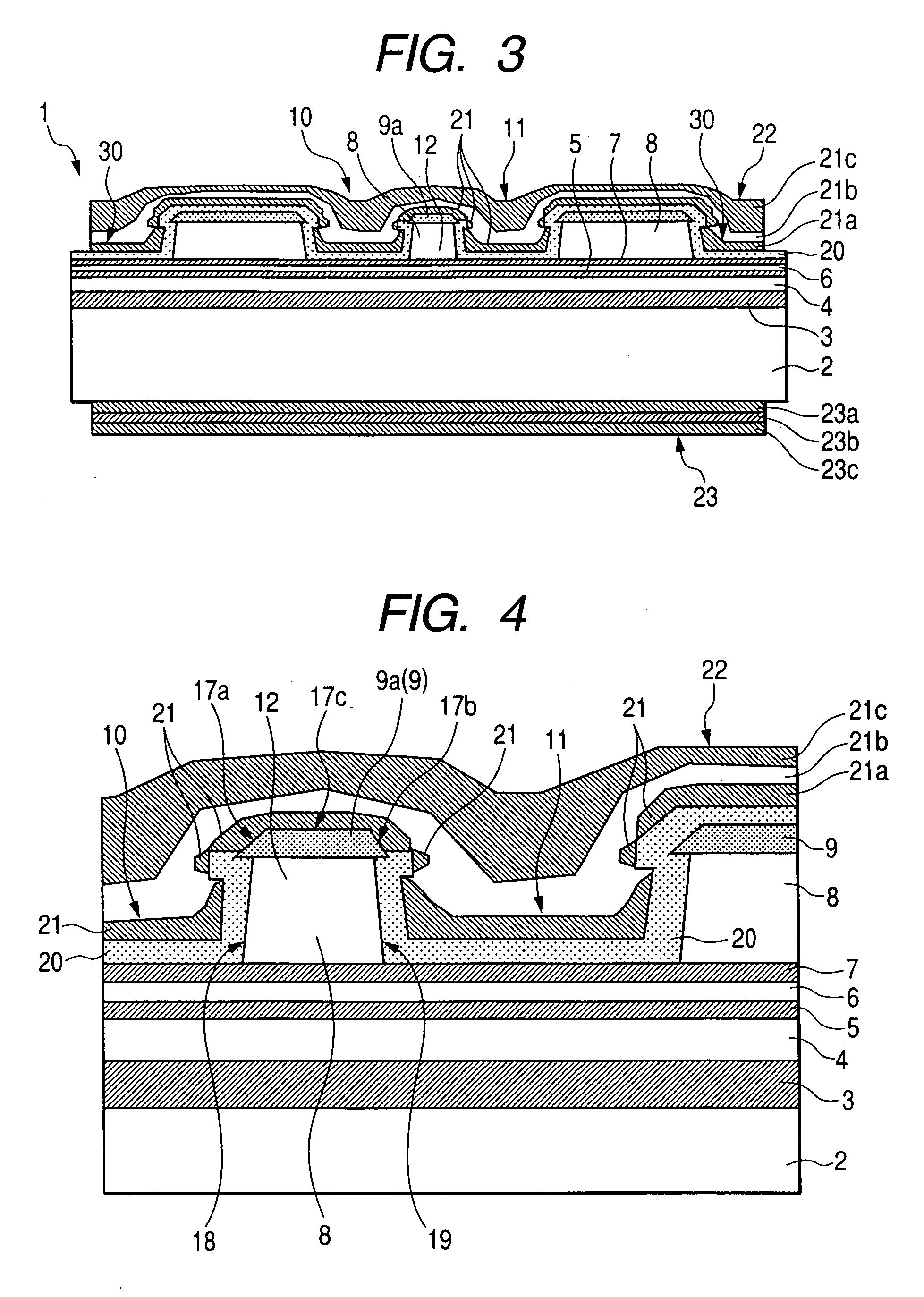
[0091] (c) Because formation of a
contact hole for electrically connecting the first
electrode (p-electrode) to the portion of the contact layer, corresponding to the ridge, is executed by etching of the insulating film by use of a self-alignment process after the
exposure and development of the contact-
resist, it is possible to form the
contact hole accurately above the ridge. It follows that the contact hole can be accurately formed even when the ridge is rendered further narrower.
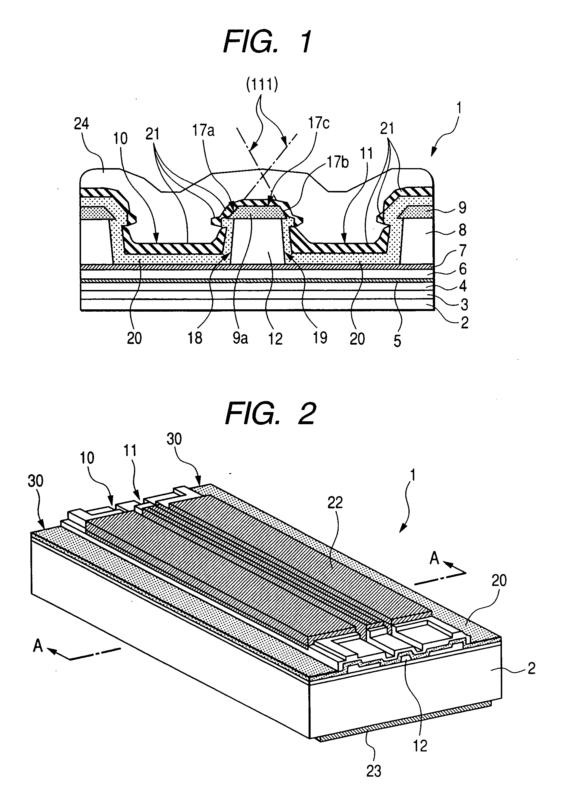
[0092] (d) Because the formation of multi-layer growth
layers on top of the semiconductor substrate is implemented by the MOCVD applied once, the number of the process steps is reduced, thereby enabling a production cost to be lowered.
[0093] (e) According to means described under item (2) as above, the semiconductor laser apparatus according to the invention is an optical semiconductor apparatus with the optical semiconductor device having a configuration described under items (1) as above, assembled inside the
package, there is no risk that gold is diffused into the ridge of the optical semiconductor device to thereby cause degradation in the characteristics thereof, so that reliability of the optical semiconductor apparatus is enhanced.

