Computer-implemented methods for detecting defects in reticle design data

a technology of design data and computer implementation, which is applied in the direction of fault response, instruments, photomechanical equipment, etc., can solve the problems of circuit decrease, defect or marginality in the features formed on the reticle becoming increasingly important, and the defect formed on the wafer during lithography may be particularly problematic for the integrated circuit manufacturing process

Active Publication Date: 2006-10-19
KLA TENCOR TECH CORP
View PDF99 Cites 131 Cited by
  • Summary
  • Abstract
  • Description
  • Claims
  • Application Information

AI Technical Summary

Benefits of technology

[0018] In one embodiment, the method may include generating an inspection process for the reticle based on results of the detecting step. In one such embodiment, the method may include linking vPWQ data to reticle inspection to drive selective sensitivity of the inspector. In an additional embodiment, the method may include generating an inspection process for the wafer based on results of the detecting step. In one such embodiment, the method may include linking vPWQ data to wafer inspection to drive selective sensitivity of the inspector. In a different embodiment, the method may include fabricating the reticle subsequent to the detecting step, inspecting the reticle, and generating an inspection process for the wafer based on results of the detecting step and the inspecting step. In this manner, the method may include linking the combination of vPWQ and reticle inspection data to wafer inspection to drive selective sensitivity of the wafer inspector. In another embodiment, the method may include fabricating the reticle subsequent to the detecting step, inspecting the reticle, and generating an inspection process for the wafer based on results of the detecting step, results of the inspecting step, critical feature data generated by a designer of the reticle design data, or some combination thereof. As such, the methods may include linking the combination of vPWQ, reticle inspection, and / or critical features identified by the designer to drive wafer inspection sensitivity, metrology sample plans and critical dimension (CD) control systems for optimal yield.

Problems solved by technology

Consequently, defects that are formed on a wafer during lithography may be particularly problematic for the integrated circuit manufacturing process.
However, as the dimensions of integrated circuits decrease and the patterns being transferred from the reticle to the wafer become more complex, defects or marginalities in the features formed on the reticle become increasingly important.
In particular, if the pattern is not formed accurately on the reticle, such discrepancies increasingly produce defects on the wafer as the dimensions of the pattern decrease and the complexity of the pattern increases.
In addition, marginalities in the reticle design may cause the design to print incorrectly on the wafer.
These efforts are relatively complex and difficult due, at least in part, to the fact that not all discrepancies or marginalities in the pattern formed on the reticle (as compared to the ideal pattern) will cause errors on the wafer that will adversely affect the integrated circuit.
In other words, some error in the pattern formed on the reticle may not produce defects on the wafer at all or may produce defects on the wafer that will not reduce the performance characteristics of the integrated circuit.
Therefore, one challenge of many in developing adequate methods and systems for qualifying a reticle pattern is to discriminate between pattern defects or marginalities that “matter” and those that do not.
However, conventional DRC operates only at the nominal process conditions, or at most, at a limited number of process conditions and / or at a limited number of points within the device.
However, this method is designed to determine only the best focus and exposure settings and not to explore the full range of the process window conditions available for each design.
Therefore, such software methods have several disadvantages.
In particular, these software methods do not exposure the full range of process window conditions thereby failing to detect process window marginalities and missing potential defects.
In addition, these methods do not determine the exact focus and exposure conditions under which defects will occur thereby preventing the complete optimization of the design.
The lack of complete process window information also limits the ability to implement advanced process control techniques for critical dimension control across all critical features on the device.

Method used


Image

  • Computer-implemented methods for detecting defects in reticle design data
  • Computer-implemented methods for detecting defects in reticle design data
  • Computer-implemented methods for detecting defects in reticle design data

Examples


Embodiment Construction

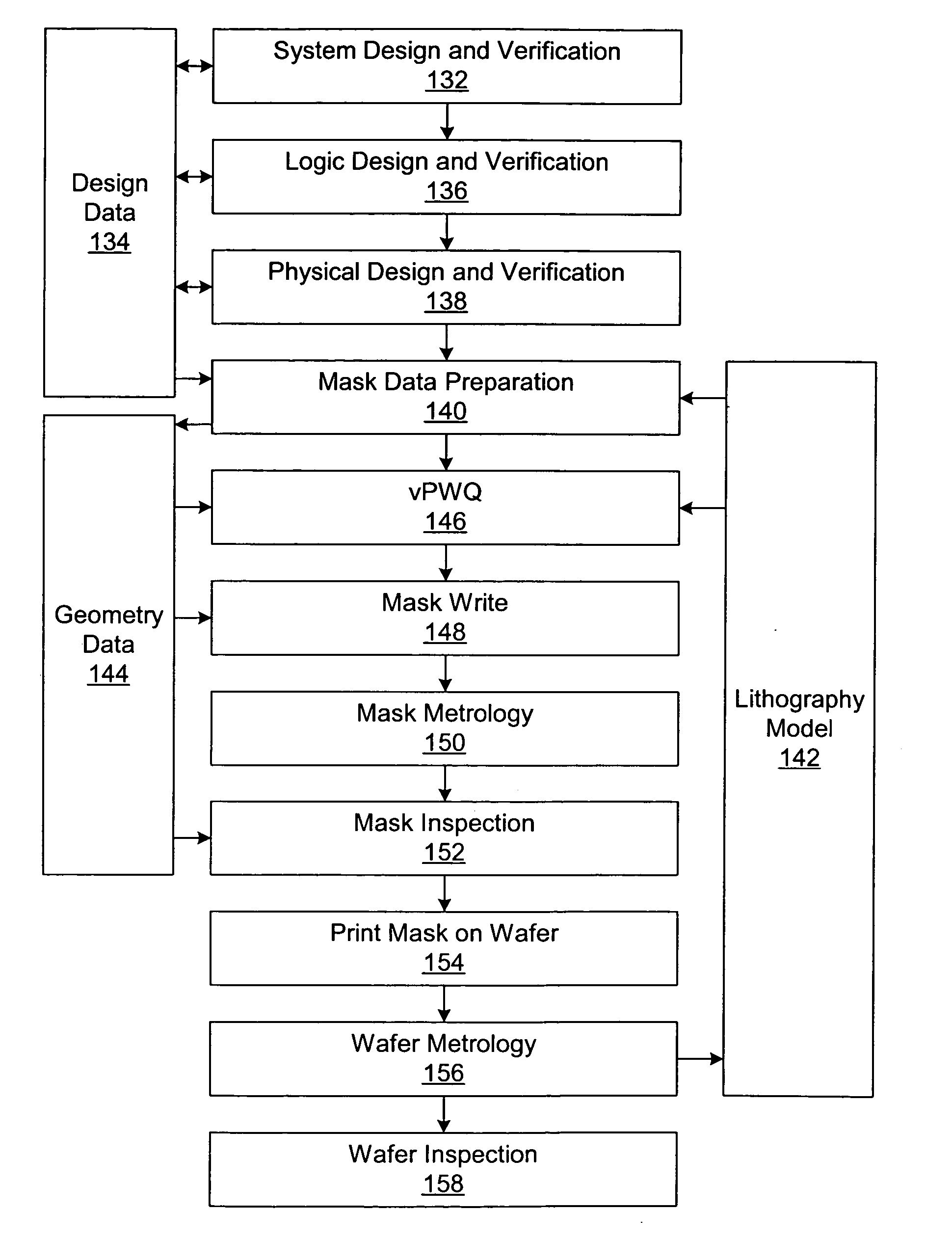
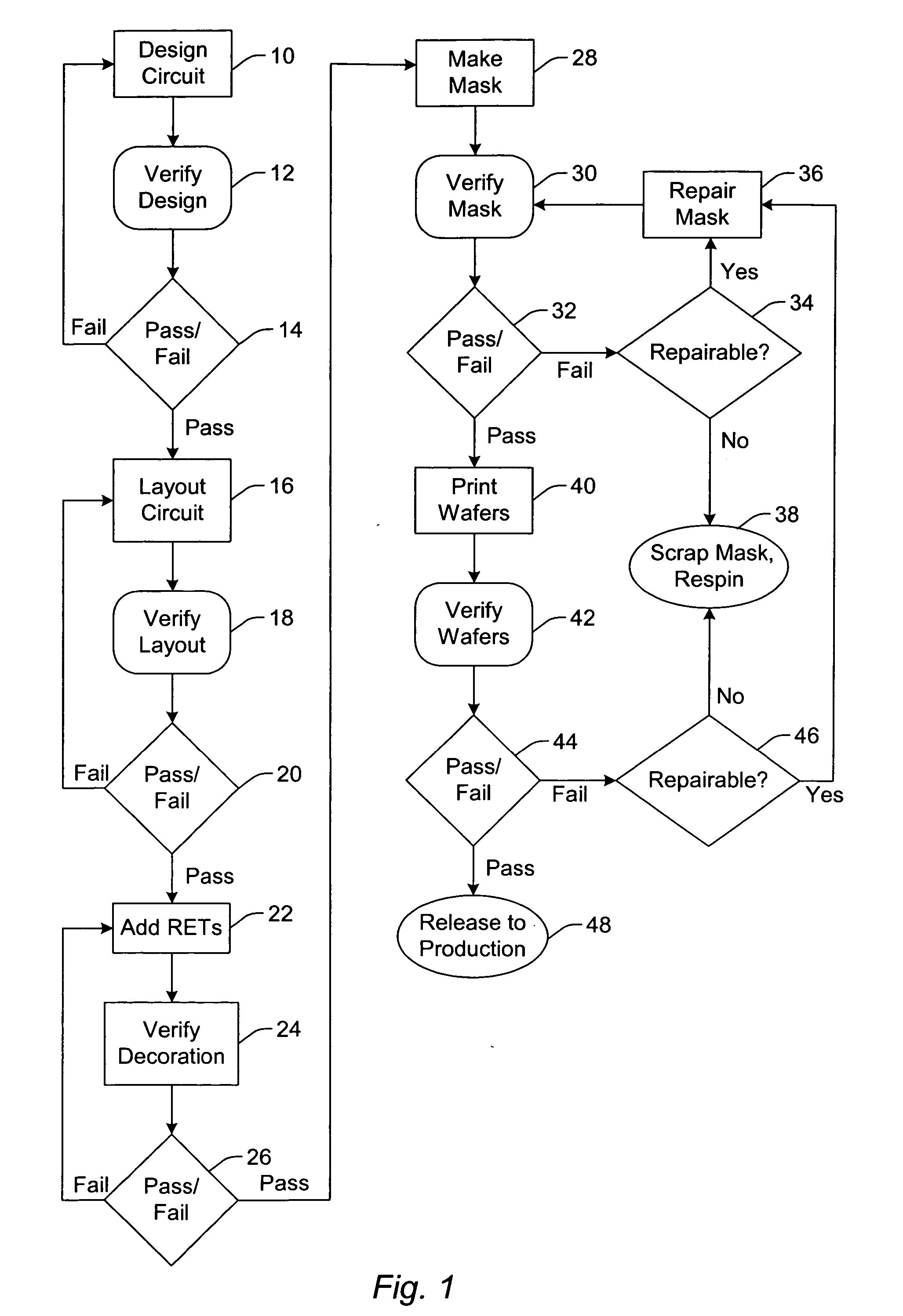
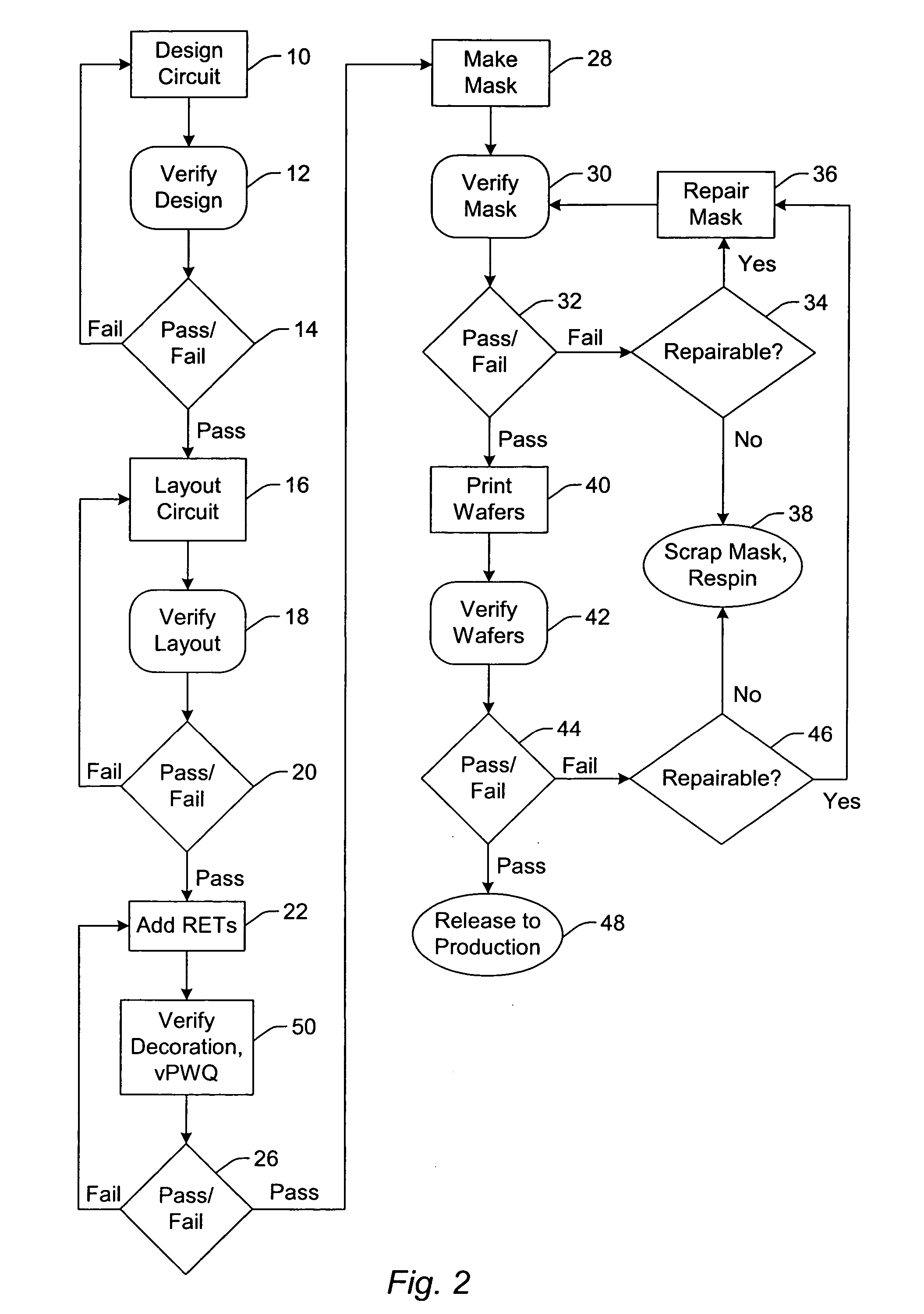
[0035] As used herein, the term “wafer” generally refers to a substrate formed of a semiconductor or non-semiconductor material. Examples of such a semiconductor or non-semiconductor material include, but are not limited to, monocrystalline silicon, gallium arsenide, and indium phosphide. Such substrates may be commonly found and / or processed in semiconductor fabrication facilities.

[0036] A wafer may include only the substrate. Such a wafer is commonly referred to as a “virgin wafer.” Alternatively, a wafer may include one or more layers formed upon a substrate. For example, such layers may include, but are not limited to, a resist, a dielectric material, and a conductive material. A resist may include any material that may be patterned by an optical lithography technique, an e-beam lithography technique, or an X-ray lithography technique. Examples of a dielectric material include, but are not limited to, silicon dioxide, silicon nitride, silicon oxynitride, and titanium nitride. A...


PUM

PropertyMeasurementUnit
defectsaaaaaaaaaa
dimensionsaaaaaaaaaa
critical dimensionaaaaaaaaaa

Abstract

Computer-implemented methods for detecting defects in reticle design data are provided. One method includes generating a first simulated image illustrating how the reticle design data will be printed on a reticle using a reticle manufacturing process. The method also includes generating second simulated images using the first simulated image. The second simulated images illustrate how the reticle will be printed on a wafer at different values of one or more parameters of a wafer printing process. The method further includes detecting defects in the reticle design data using the second simulated images. Another method includes the generating steps described above in addition to determining a rate of change in a characteristic of the second simulated images as a function of the different values. This method also includes detecting defects in the reticle design data based on the rate of change.

Description

PRIORITY CLAIM [0001] This application claims priority to U.S. Provisional Application No. 60 / 540,031 entitled “Method and System of Qualifying Integrated Circuit Design for Manufacturability and Application to Improving Critical Dimension Control in Integrated Circuit Manufacturing,” filed Jan. 29, 2004.BACKGROUND OF THE INVENTION [0002] 1. Field of the Invention [0003] The present invention generally relates to computer-implemented methods for detecting defects in reticle design data. Certain embodiments relate to a computer-implemented method that includes detecting defects in reticle design data using simulated images that illustrate how a reticle will be printed on a wafer at different values of one or more parameters of a wafer printing process. [0004] 2. Description of the Related Art [0005] The following descriptions and examples are not admitted to be prior art by virtue of their inclusion within this section. [0006] Fabricating semiconductor devices such as logic and memor...

Claims


Application Information

Patent Timeline
Patent Type & Authority Applications(United States)
IPC IPC(8): G06F17/50G03F1/00G03F7/20
CPCG03F1/144G03F1/36G03F1/84G03F7/70433G03F7/70441G06Q30/0206G03F7/70533G03F7/70616G03F7/7065G03F7/70666G03F7/705G06F11/22G06F11/08G06F11/00
Inventor SAIDIN, ZAIN K.XIONG, YALINGLASSER, LANCEHESS, CARLPREIL, MOSHE E.
Owner KLA TENCOR TECH CORP
Why Eureka
Try Eureka