High electron mobility transistor (HEMT) structure with refractory gate metal

a high electron mobility, transistor technology, applied in the field of hemts, can solve the problems of reducing the height of the schottky barrier, increasing the current of the reverse gate, and adversely affecting performance, so as to improve the long-term reliability of the inp hemt and achieve superior performance.

Active Publication Date: 2006-11-02
NORTHROP GRUMMAN SYST CORP
View PDF5 Cites 11 Cited by
  • Summary
  • Abstract
  • Description
  • Claims
  • Application Information

AI Technical Summary

Benefits of technology

[0010] It will be appreciated from the foregoing that the present invention represents a significant advance in InP HEMT technology. In particular, with a simple, but critical, change in gate metal structure the invention improves the long-term reliability of InP HEMTs wit

Problems solved by technology

In terms of electrical characteristics of the gate junction, the interdiffusion of titanium results in an increase of revers

Method used


Image

  • High electron mobility transistor (HEMT) structure with refractory gate metal
  • High electron mobility transistor (HEMT) structure with refractory gate metal
  • High electron mobility transistor (HEMT) structure with refractory gate metal

Examples


Embodiment Construction

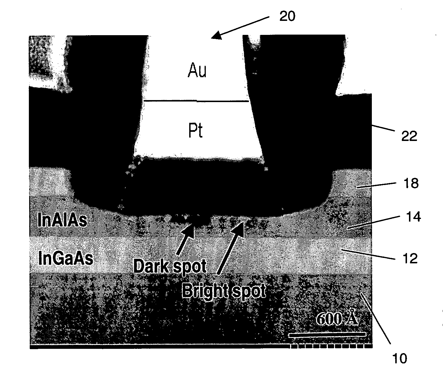
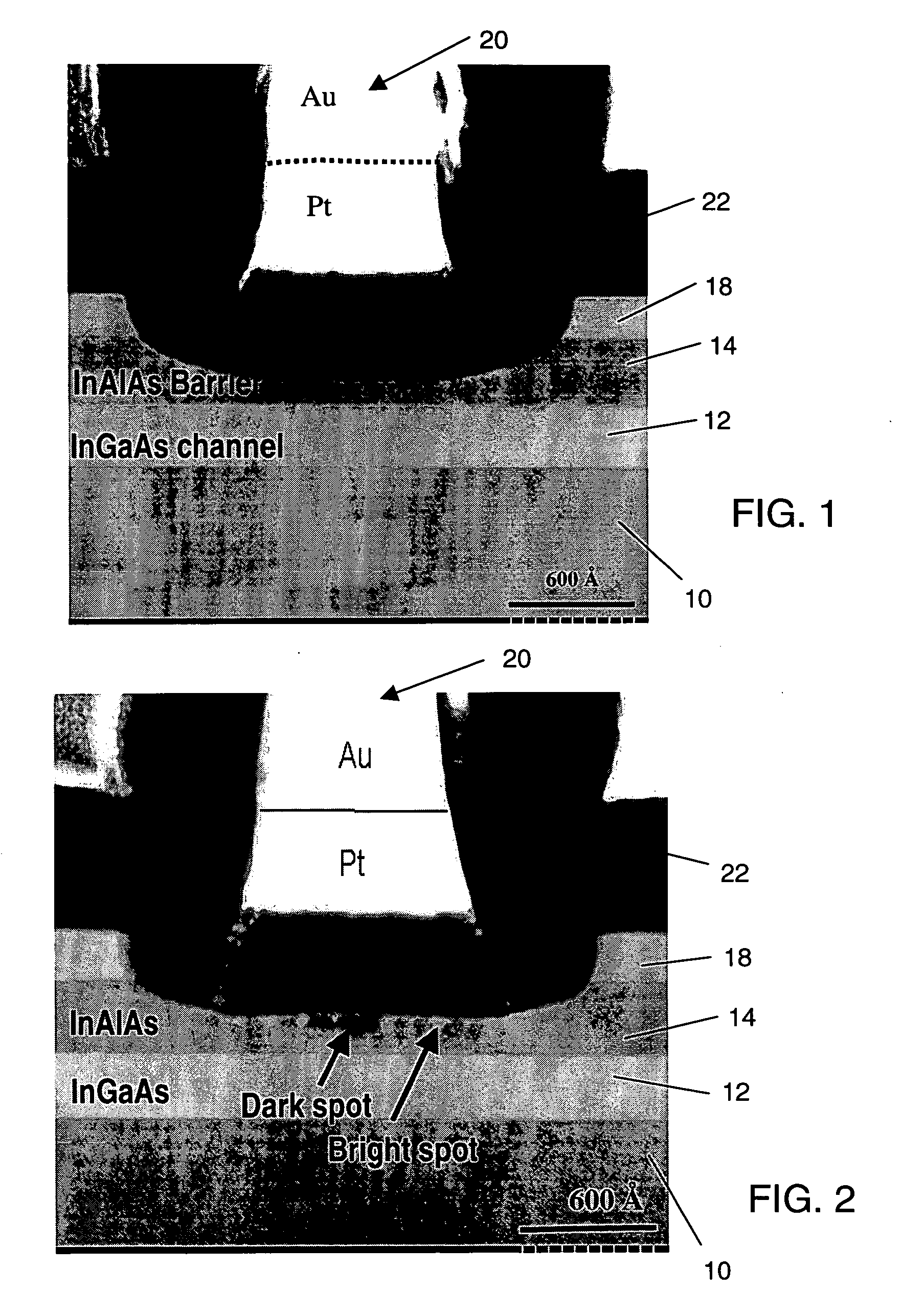
[0018] As shown in the drawings for purposes of illustration, the present invention is concerned with high electron mobility transistors (HEMTs) and, more particularly, with HEMTs employing indium phosphide (InP) and related materials. Prior to this invention InP HEMT devices, whether implemented as discrete devices or in integrated circuits such as microwave monolithic integrated circuits (MMICs), have typically included a gate metal structure consisting of three successive layers of titanium (Ti), platinum (Pt) and gold (Au). While it has been widely recognized that InP HEMTs have superior performance at microwave and millimeter wave frequencies, a known disadvantage of the devices is a potential to exhibit degradation in performance over long-term use.

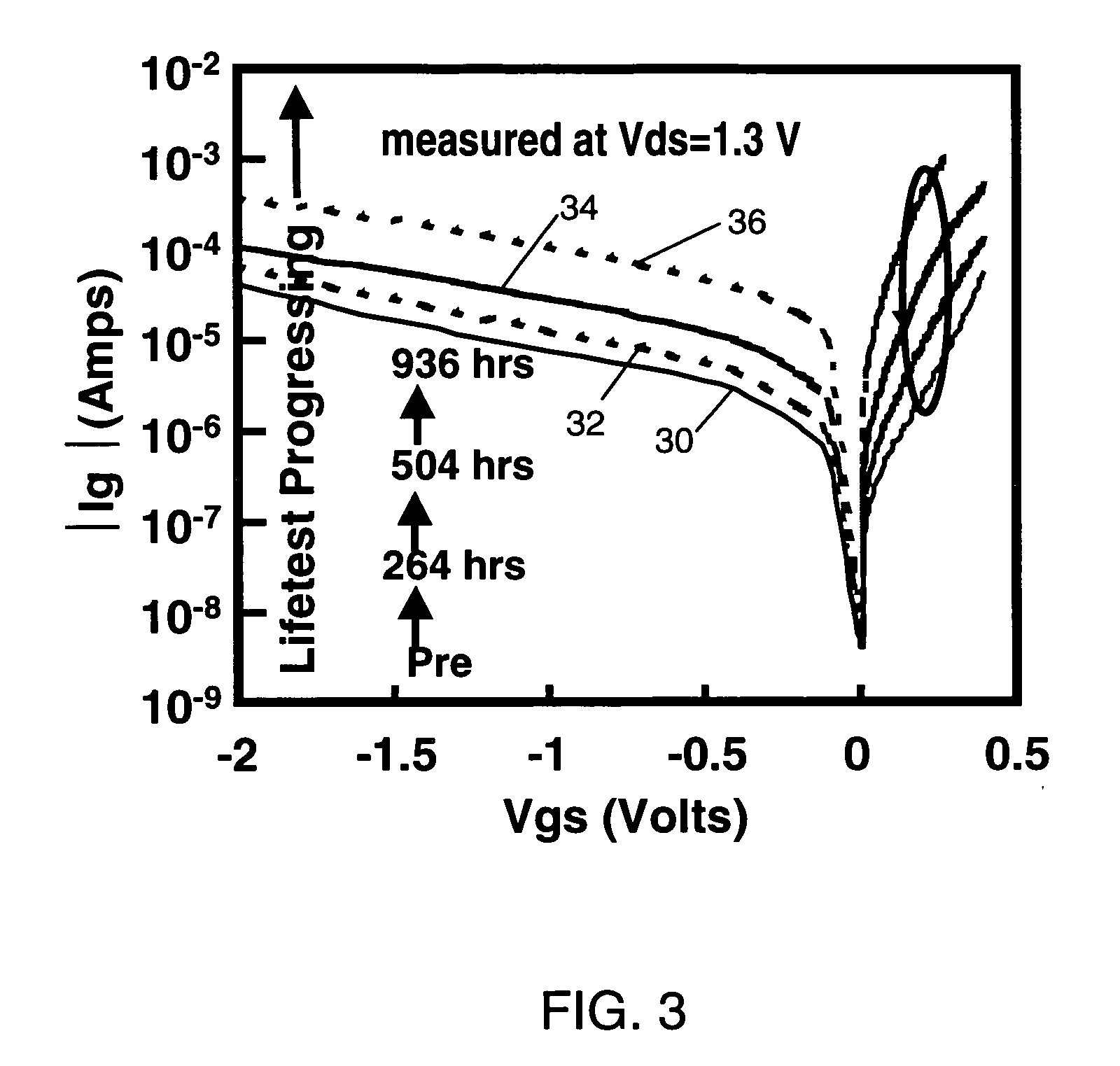
[0019] In the past, long-term performance degradation of InP HEMTs has been attributed a variety of degradation mechanisms. Recently, however, it has been shown by the present inventors that degradation of the Schottky junction bet...


PUM


Abstract

An InP high electron mobility transistor (HEMT) structure in which a gate metal stack includes an additional thin layer of a refractory metal, such as molybdenum (Mo) or platinum (Pt) at a junction between the gate metal stack and a Schottky barrier layer in the HEMT structure. The refractory metal layer reduces or eliminates long-term degradation of the Schottky junction between the gate metal and the barrier layer, thereby dramatically improving long-term reliability of InP HEMTs, but without sacrifice in HEMT performance, whether used as a discrete device or in an integrated circuit.

Description

BACKGROUND OF THE INVENTION [0001] This invention relates generally to high electron mobility transistor (HEMT) structures and, more particularly, to HEMTs using indium phosphide (InP) and related materials. A HEMT is a type of field effect transistor (FET) in which current flow between two terminals, referred to as the source and drain terminals, is controlled by a voltage applied to a gate terminal. HEMTs are widely used in a variety of applications, but particularly as low noise amplifiers operating at microwave and millimeter wave frequencies. HEMTs may be implemented as discrete transistors or in integrated circuits, such as microwave monolithic integrated circuits (MMICs) in space, military and commercial applications. [0002] The present invention is particularly concerned with a known disadvantage of the InP HEMT, which includes, for example, a channel layer of indium gallium arsenide (InGaAs) and a barrier layer of indium aluminum arsenide (InAlAs) formed over an InP substra...

Claims


Application Information

Patent Timeline
IPC IPC(8): H01L29/739
CPCH01L29/42316H01L29/7783H01L29/475
Inventor CHOUG, YEONG-CHANGGRUNDBACHER, RONALDLIU, PO-HSINLEUNG, DENISE L.LAI, RICHARD
Owner NORTHROP GRUMMAN SYST CORP
Why Eureka
Try Eureka