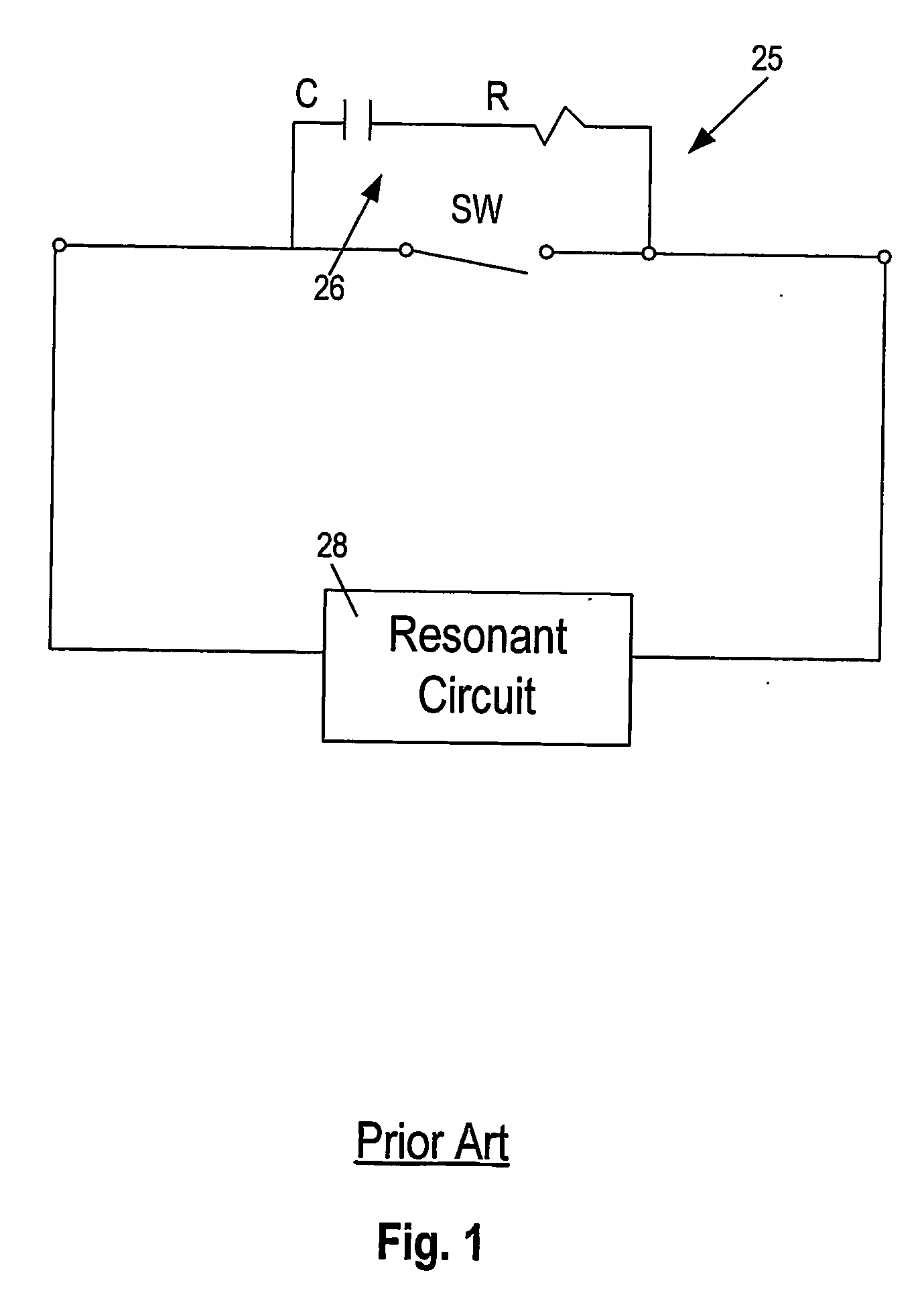
Active snubber

a snubber and active technology, applied in the direction of efficient power electronics conversion, electric variable regulation, instruments, etc., can solve the problems of increasing the cost of components, requiring larger diodes, and ringing in the primary and secondary circuits of transformers, so as to achieve less power dissipation

Inactive Publication Date: 2006-11-02
DET INT HLDG LTD
View PDF3 Cites 21 Cited by
  • Summary
  • Abstract
  • Description
  • Claims
  • Application Information

AI Technical Summary

Benefits of technology

[0012] Preferably, in accordance with a preferred embodiment of the invention, the resistance of the RC snubber circuit is close to the characteristic impedance of the parasitic resonant circuit that the snubber serves. In one preferred embodiment of the invention, the electrically controlled switch is a MOSFET device in series with the RC circuit that is the snubber. The electrically controlled switch can be, however, any of a number of fast switching devices including NPN or PNP discrete transistors, a CMOS transistor, either discrete or integrated, an SCR or any other precisely electrically controlled fast switch or switching device. Further, in accordance with a preferred embodiment of the invention, the electrically controlled switch completes a current path during each abrupt voltage increase in the resonant circuit to cause charging of the capacitor of the snubber to begin before the first spike or resonant overshoot occurs across the primary switch. The electrically controlled switch then interrupts the current path to the charged snubber capacitor to prevent its complete discharge. Subsequently, the capacitor is not charged from a totally discharged state to its fully charged state and is, in use, never completely discharged. Rather, the capacitor has held a large part of its charge and little current is required to recharge it during the snubber's damping. Consequently, there is considerably less power dissipation in the resistor of the snubber circuit.

Problems solved by technology

In power devices such as DC-DC converters, abrupt voltage changes can result in transient ringing in the primary and secondary circuits of a transformer.
This can exceed the diode maximum voltage rating, or it may require larger, more expensive components than would be needed in the absence of such overvoltage.
However, the damping should be optimized since an excessive damping will increase the switching time and switching losses will become more significant.
The main disadvantage of this usual snubber 25 is the power lost cycle by cycle to charge the capacitor of the snubber from zero to the maximum value of the overvoltage across the switch.
Depending on the value of the voltage swing, these losses may become significant for power devices such as high efficiency DC-DC converters.

Method used


Image

  • Active snubber
  • Active snubber
  • Active snubber

Examples


Embodiment Construction

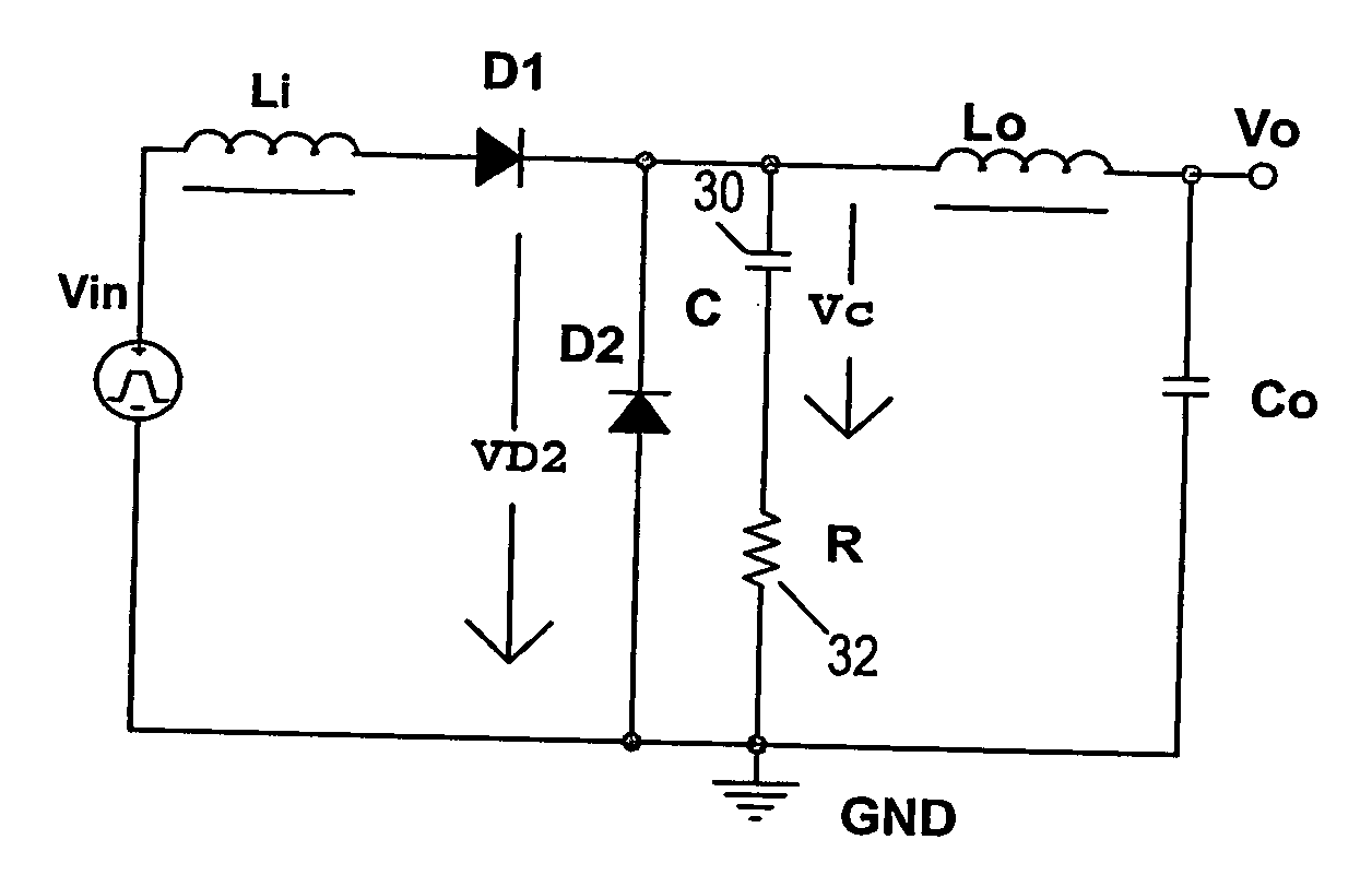
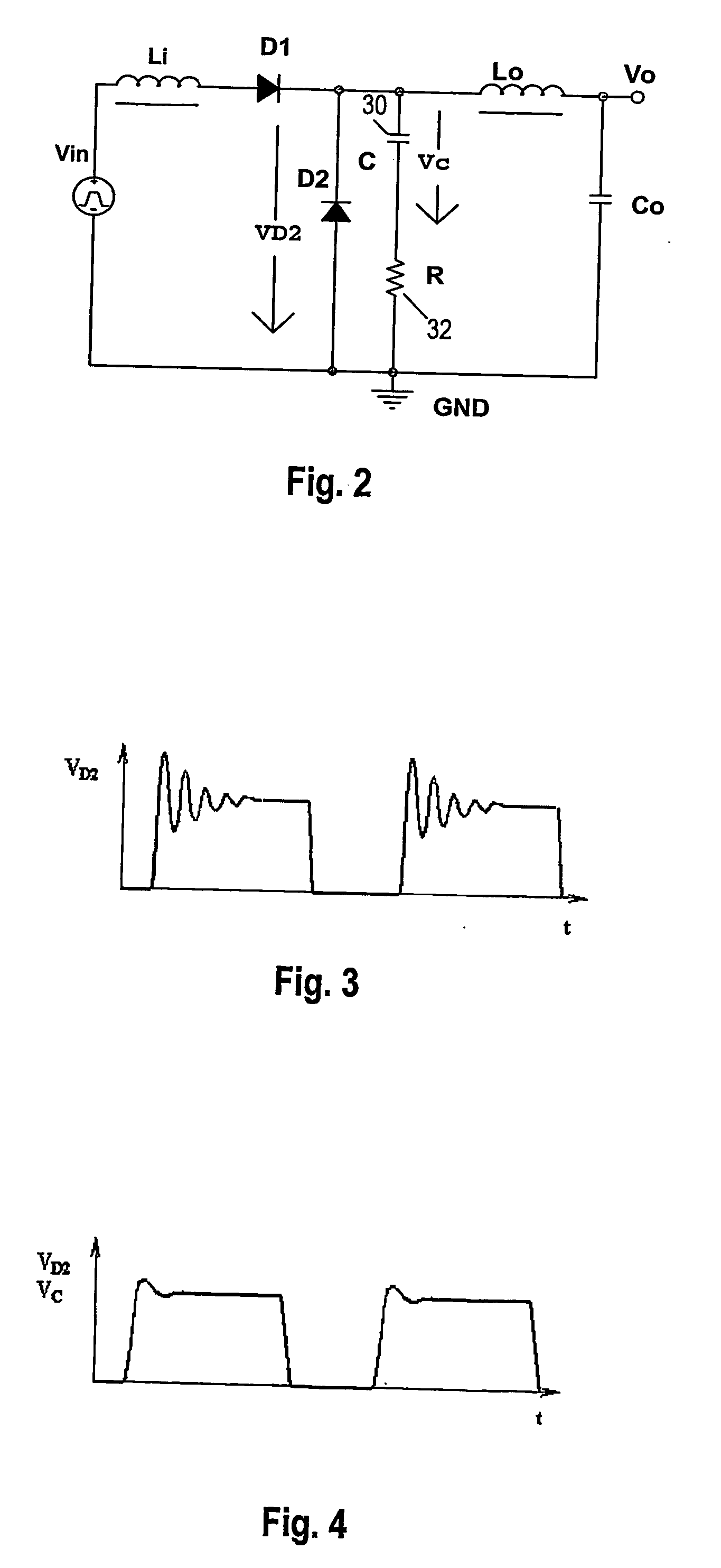
[0029] Turning now to FIG. 5, a generalized resonant circuit 40 is shown there in accordance with the prior art. An input voltage Vin is applied at 42. The input voltage has abrupt rise and fall times and is of the nature of a square wave as shown. In FIG. 6, the input voltage is depicted with an abrupt rise time at time T. The circuit 40 has an inductance Lp as would a power device with a transformer primary 44 to be driven by the input voltage Vin. A capacitor 46 has a capacitance Cp which could be, for example, parasitic capacitance in the circuit 40. The inductance Lp and capacitance Cp, then, form a resonant tank circuit. An output rectifier diode 48 switches from its non-conducting to its conducting state responsive to Vin. Current in the diode 48 is plotted at 50 in FIG. 6. Ringing is apparent at turn-on in the region 52. Ringing is likewise apparent in the plot 54 of Vp versus time in the region 56. Spiking at the outset of turn-on causes stress on the diode 48 to be almost ...


PUM


Abstract

An improved snubber is electrically switched to close a current path to a capacitor (C) in a series connected RC circuit at the onset of an abrupt voltage change otherwise producing ringing in a resonant circuit to which the snubber circuit is connected. The current path to the capacitor (C) is then interrupted before the capacitor (C) discharges and thereafter at each such voltage change in the resonant circuit the capacitor (C) is no longer charged from its totally discharged state but nevertheless damps the ringing by virtue of current flow to the nearly completely charged capacitor (C). By preventing complete charging and discharging of the capacitor (C) in the RC circuit every cycle, power dissipation in the resistance of the snubber circuit is greatly reduced.

Description

BACKGROUND OF THE INVENTION [0001] This invention relates to circuit provisions for damping resonant ringing in an electrical circuit, and more particularly to a switched RC circuit connected with a resonant circuit to damp ringing. [0002] In power devices such as DC-DC converters, abrupt voltage changes can result in transient ringing in the primary and secondary circuits of a transformer. For example, for a regular DC-DC converter, the rectification in a power transformer secondary uses one or more ultra fast or Schottky rectifiers. The leakage inductance of the transformer may interact resonantly with the reverse recovery current and / or with the junction capacitance of the output rectifier diode(s). The leakage inductance and the junction capacitance together with all the parasitic inductances and capacitances of the layout determine the resonant frequency. This resonant circuit has low losses. As a result, many cycles of ringing will occur after the first spike. Also, the ringin...

Claims


Application Information

Patent Timeline
Patent Type & Authority Applications(United States)
IPC IPC(8): G05F1/00H02M1/34H02M3/155H03K17/0814
CPCH02M1/34H02M3/155H02M2001/344H03K17/74H03K17/0814H03K17/687H03K17/04Y02B70/10H02M1/342H02M1/344
Inventor JITARU, IONEL D.CASARU, GEORGE
Owner DET INT HLDG LTD
Why Eureka
Try Eureka