Method For Manufacturing Nitrogen-Doped Silicon Single Crystal

a silicon single crystal and nitrogen-doped technology, applied in the direction of crystal growth process polycrystalline material growth, etc., can solve the problems of reducing production yield, silicon single crystals can suddenly become weak against thermal stress, and affecting mechanical strength, so as to achieve the effect of increasing nitrogen concentration

Inactive Publication Date: 2006-11-16
SUMCO CORP
View PDF5 Cites 8 Cited by
  • Summary
  • Abstract
  • Description
  • Claims
  • Application Information

AI Technical Summary

Benefits of technology

[0020] As described above, according to the present invention, there is provided an improvement in a method for manufacturing a silicon single crystal in which nitrogen is doped at a rate which is not smaller than 1×10¹⁵ atoms / cm3 and less than 4.5×10¹⁵ atoms / cm3 by pulling up the silicon single crystal from a silicon melt containing nitrogen stored in a quartz crucible, wherein the silicon single crystal is pulled up while supplying a silicon raw material which does not contain nitrogen into the silicon melt in such a manner that a liquid level position of the silicon melt stored in the quartz crucible is maintained constant in accordance with the growth amount of the single crystal.
[0021] According to this method, an increase in nitrogen concentration in the silicon melt due to a segregation phenomenon of nitrogen caused by pulling up the single crystal can be suppressed while additionally supplying the silicon raw material, thereby growing a silicon single crystal having a uniform nitrogen concentration region in an axial direction.

Problems solved by technology

In the CZ method, therefore, a part of the quartz glass of the crucible which comes into contact with the silicon melt unavoidably melts into the silicon melt, whereby oxygen is blended in the melt.
The impurity oxygen seriously affects mechanical strength, a defect induced by a heat treatment and internal gettering of a silicon wafer obtained by slicing the silicon single crystal.
However, a phenomenon occurs in that the silicon single crystal can suddenly become weak against thermal stress when the impurity oxygen has precipitated in the silicon single crystal.
Additionally, it can cause a leak or the like at an element isolation part, thereby reducing the production yield.
Therefore, there is a problem in that nitrogen cannot be uniformly doped in the grown silicon single crystal.
In method (2), it is hard to control the flow quantity of nitrogen or the nitrogen compound gas, and the nitrogen doping amount may possibly increase in the vicinity of the surface of the pulled-up silicon single crystal.
Therefore, there is a problem that the pull-up length with which growth is enabled is limited.

Method used


Image

  • Method For Manufacturing Nitrogen-Doped Silicon Single Crystal
  • Method For Manufacturing Nitrogen-Doped Silicon Single Crystal
  • Method For Manufacturing Nitrogen-Doped Silicon Single Crystal

Examples


example 1

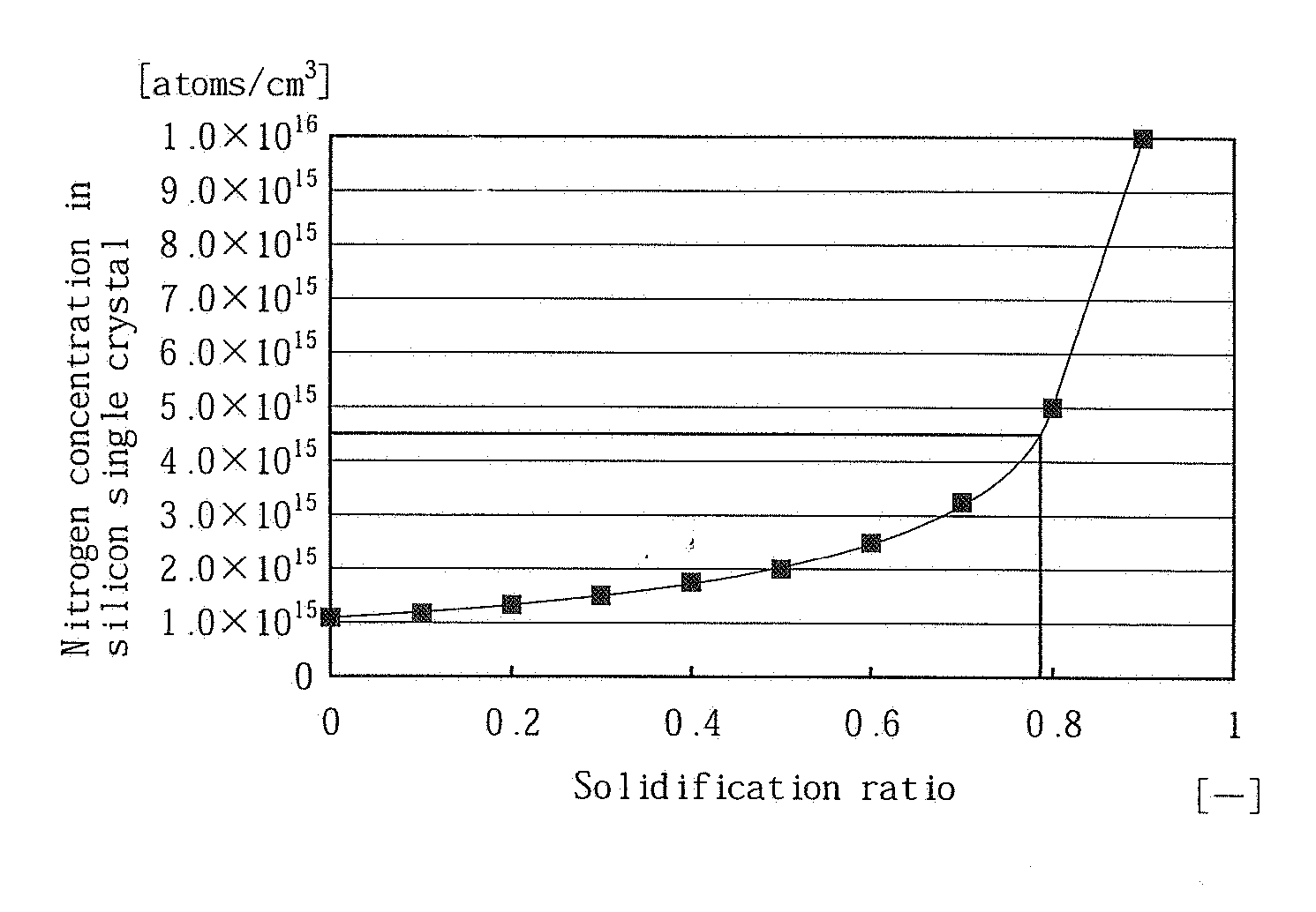
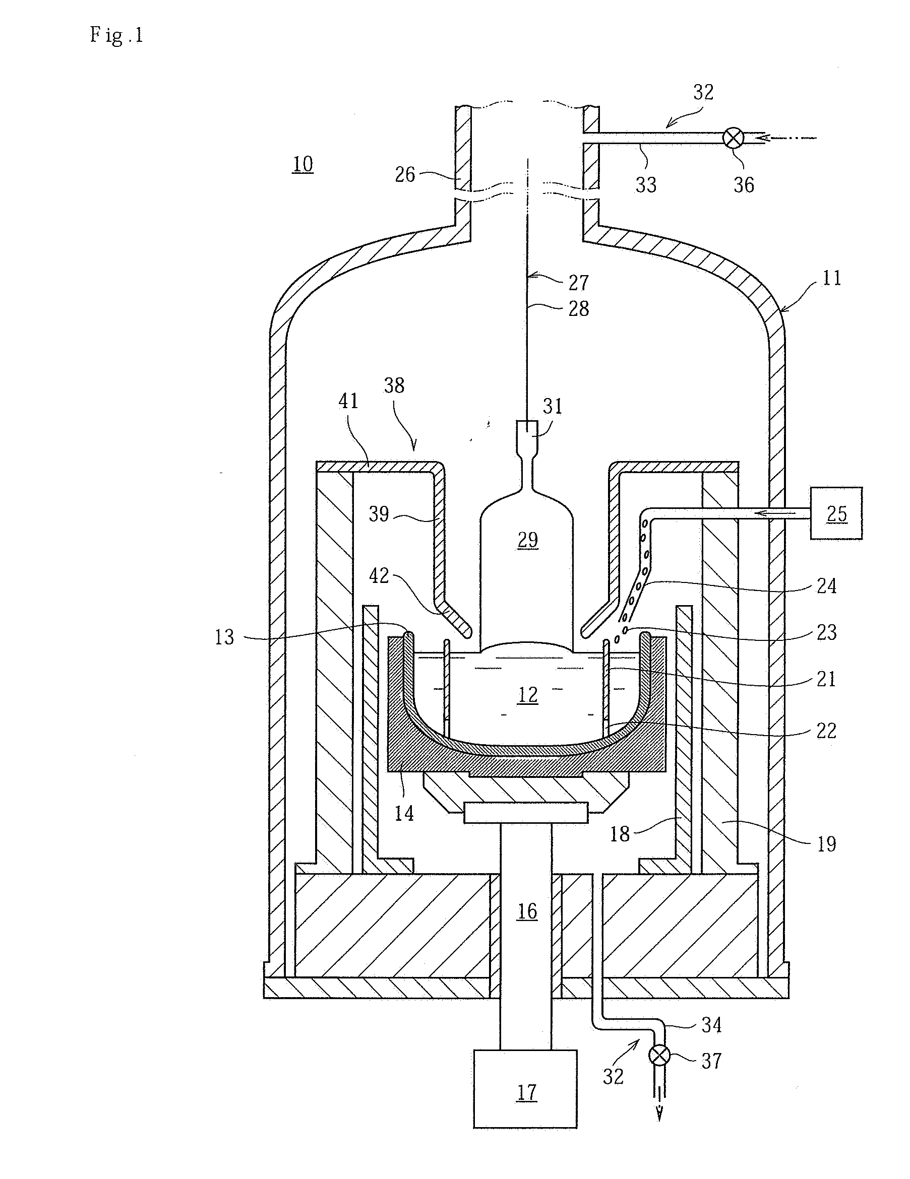
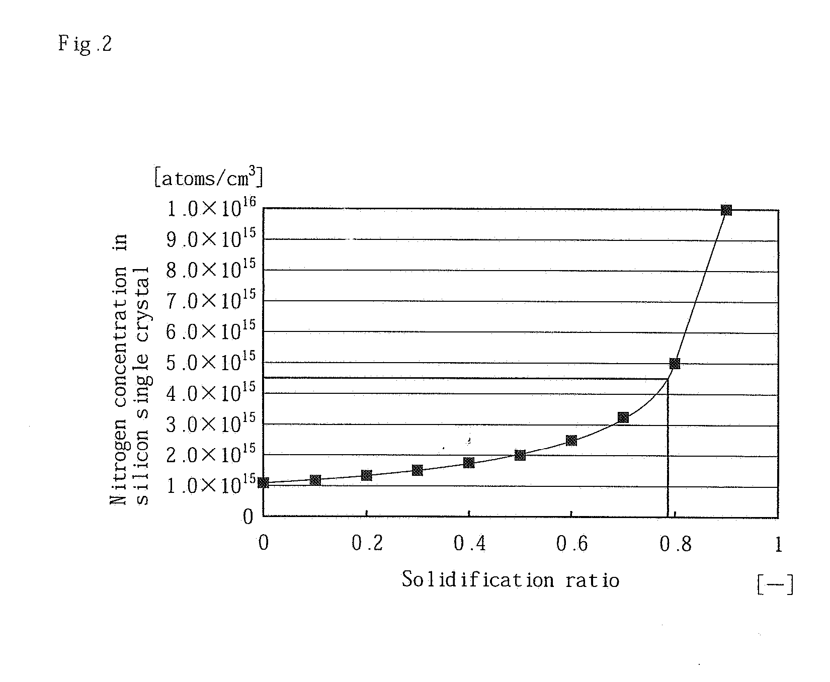
[0036] 80 kg of a silicon melt containing nitrogen at a rate of 1.43×10¹⁵ atoms / cm3 was stored in a quartz crucible. Furthermore, 80 kg of a silicon raw material which does not contain nitrogen was prepared. Then, a seed crystal was dipped in the silicon melt, and this seed crystal was pulled upward while gently rotating to start growth of a silicon single crystal having a diameter of 8 inches (approximately 200 mm). The silicon raw material which does not contain nitrogen was continuously supplied into the silicon melt without moving the quartz crucible up and down in such a manner that the liquid level position of the silicon melt stored in the quartz crucible is maintained constant in accordance with the amount of growth of the single crystal until 80 kg of the silicon single crystal is grown. Subsequently, after stopping supply of the silicon raw material, the silicon single crystal was grown while moving the quartz crucible up in such a manner that the liquid level position of ...


PUM

PropertyMeasurementUnit
diameteraaaaaaaaaa
diameteraaaaaaaaaa
lengthaaaaaaaaaa

Abstract

There is provided an improvement in a method for manufacturing a silicon single crystal in which nitrogen is doped at a rate which is not smaller than 1×10¹⁵ atoms/cm3 and less than 4.5×10¹⁵ atoms/cm3 by pulling up a silicon single crystal 29 from a silicon melt 12 which is stored in a quartz crucible 13 and contains nitrogen, wherein the single crystal is pulled up while supplying a silicon raw material 23 which does not contain nitrogen into the silicon melt 12 in such a manner that the liquid level position of the silicon melt stored in the quartz crucible is maintained constant in accordance with the amount of growth of the single crystal. The amount of nitrogen contained in a pulled-up silicon single crystal is controlled, and hence a uniform nitrogen concentration can be obtained along the axial direction of the single crystal. The pull-up length of the silicon single crystal in which nitrogen is doped at a high concentration can be increased.

Description

BACKGROUND OF THE INVENTION [0001] 1. Field of the Invention [0002] The present invention relates to a method for manufacturing a silicon single crystal in which nitrogen is doped based on a Czochralski method (which will be referred to as a CZ method hereinafter). [0003] 2. Description of the Related Art [0004] In the CZ method, polycrystal silicon is melted in a crucible formed of amorphous quartz glass, and a seed crystal which has been brought into contact with the upper surface of the silicon melt is pulled up while gently rotating. The silicon melt which contacts the seed crystal loses its heat through the seed crystal and is crystallized with the crystal orientation of the seed crystal when the molten silicon solidifies on the seed crystal, and is pulled up as a silicon single crystal. In the CZ method, therefore, a part of the quartz glass of the crucible which comes into contact with the silicon melt unavoidably melts into the silicon melt, whereby oxygen is blended in the ...

Claims


Application Information

Patent Timeline
Patent Type & Authority Applications(United States)
IPC IPC(8): C30B15/00C30B21/06C30B27/02C30B28/10C30B30/04
CPCC30B15/04C30B29/06C30B15/30C30B15/12H01L21/20
Inventor FURUKAWA, JUNHARADA, KAZUHIRO
Owner SUMCO CORP
Why Eureka
Try Eureka