Low crosstalk substrate for mixed-signal integrated circuits

a technology of integrated circuits and substrates, which is applied in the direction of semiconductor devices, electrical equipment, semiconductor/solid-state device details, etc., can solve the problems of noise-sensitive circuit elements, single-chip radio frequency integrated circuits, etc., and achieve enhanced heat sinking and improved crosstalk isolation

Active Publication Date: 2006-11-16
RGT UNIV OF CALIFORNIA
View PDF4 Cites 8 Cited by
  • Summary
  • Abstract
  • Description
  • Claims
  • Application Information

AI Technical Summary

Benefits of technology

[0011] The present invention generally comprises an integrated circuit laminate with a metal substrate for high performance mixed signal integrated circuit applications. The metal substrate provides substantially improved crosstalk isolation, enhanced heat sinking and an easy access to true low impedance ground. One of the major obstacles of the production of single chip radio frequency integrated circuits is noise from switching transients in digital cir

Problems solved by technology

One of the major obstacles of the production of single chip radio frequency integrated circuits is noise from switching transients in digita

Method used


Image

  • Low crosstalk substrate for mixed-signal integrated circuits
  • Low crosstalk substrate for mixed-signal integrated circuits
  • Low crosstalk substrate for mixed-signal integrated circuits

Examples


example 1

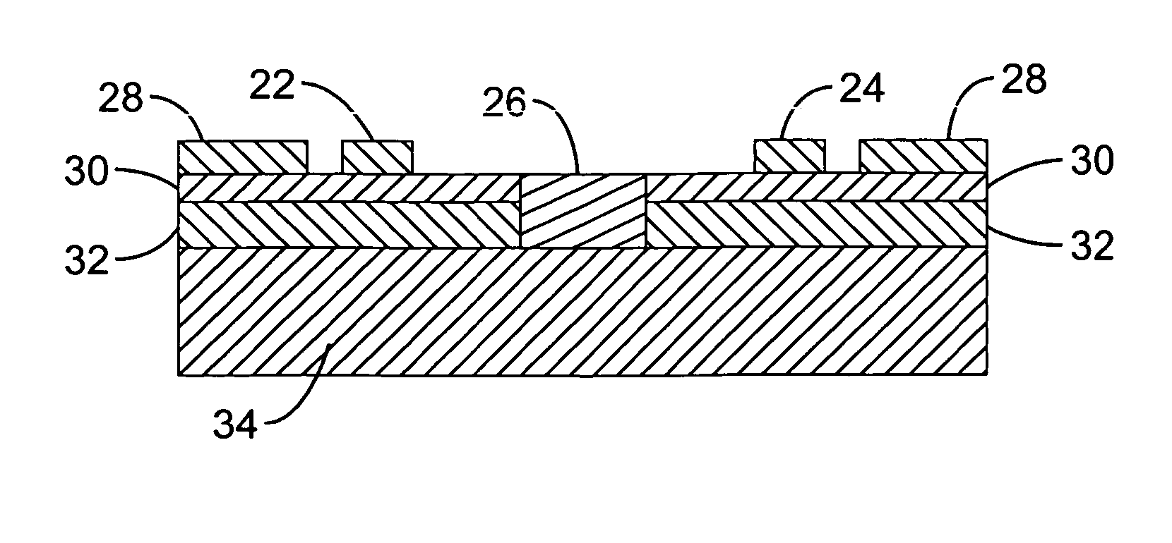
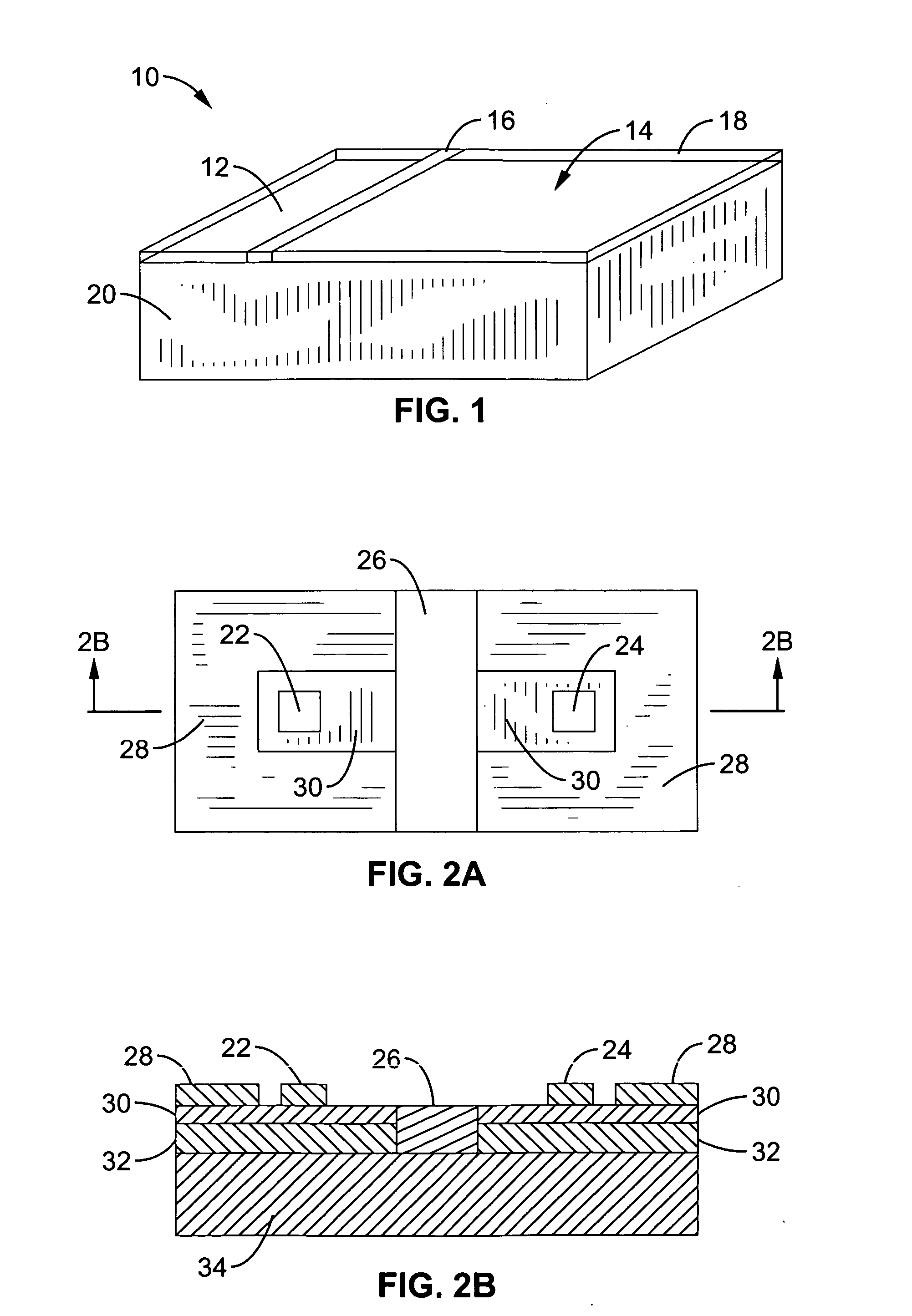
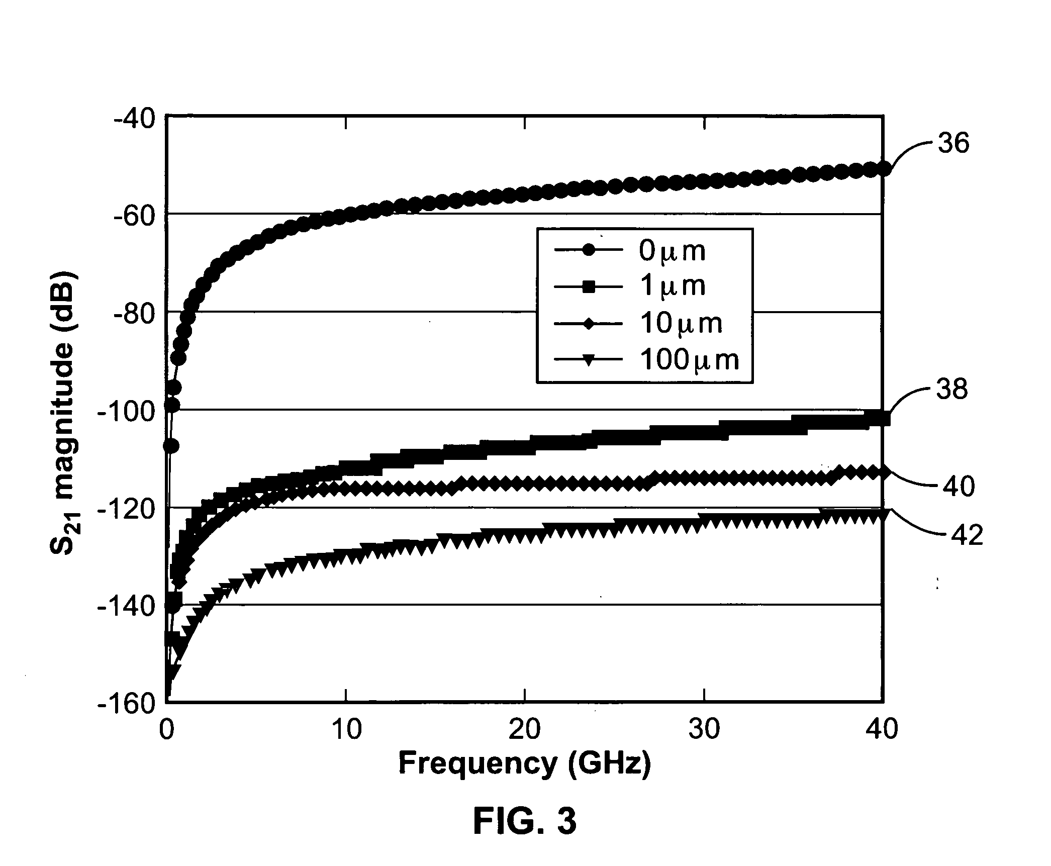
[0060] A preliminary test of the concept of crosstalk isolation was conducted using a test chip configuration shown in top and cross-sectional views inFIG. 2A and FIG. 2B. The chip was configured with two metal pads 22 and 24 separated by a metal trench 26. The pads 22 and 24 and the ground plane 28 are approximately 5000 angstroms thick aluminum and the pads were square shaped with 100 μm×100 μm sides. A distance of approximately 800 μm separated the pads 22 and 24. The metal trench 26 is physically and electrically connected to the grounding plane 28.

[0061] As seen in the cross-section of FIG. 2B, the pads 22, 24 and ground plane 28 are disposed on a dielectric layer 30 that is preferably composed of PECVD SiO2. The dielectric layer is approximately 5000 angstroms thick in this example.

[0062] A substrate layer 32 of (p-) Silicon about 2 μm thick with approximately 10 Ω-cm resistivity was attached to a metal plate 34 on the bottom side and the dielectric layer 30 on the top side ...

example 2

[0065] Capacitive and electromagnetic coupling between the inductor and the metal substrate may limit the inductor performance and restrict design freedom. However this coupling can be overcome with insulator filled pockets in the metal substrate under the inductor. Turning now to FIG. 4A and FIG. 4B, an on-chip inductor structure for a 4 nH inductor is shown. The inductor 44 has 5.5 turns with segment 46 width of 12 μm and the space 48 between the segments 46 was 4 μm. The inner dimension of the inductor 44 was 60 μm and the outer dimension of the inductor was 232 μm. The height of the segments 46 of inductor spiral 44 was 40,000 angstroms.

[0066] As seen in FIG. 4B, the metal spiral of the inductor 44 is disposed on a 10,000-angstrom layer 50 of PECVD oxide. A metal underpass 60 that is approximately 5000 angstroms thick joins the center of the inductor to pad 62. A second layer 52 of PECVD oxide approximately 20,000 angstroms in thickness is disposed between the first oxide layer...

example 3

[0068] At the present time, flexible electronics are limited to low performance systems based on soft materials such as conducting polymers. It has been shown that hard materials can have a range of flexibility if the material is sufficiently thin. For example, commercially available 50 μm thick silicon wafers of several inches in diameter have limited flexibility similar to a credit card.

[0069] The thin silicon and copper bi-film of the present invention can also be used to provide high performance flexible integrated circuits. In one embodiment, the silicon and copper films are attached to a flexible plastic card using a stress relieving soft material that allows the bi-film to slightly glide relative to the plastic card. The function of the card is to support the films and restrict the maximum bending radius and provide the necessary mechanical integrity. The pliant stress relief layer is necessary to allow the Si—Cu bi film to bend relative to its center as opposed to that of t...


PUM


Abstract

An integrated circuit laminate with a metal substrate for use with high performance mixed signal integrated circuit applications. The metal substrate provides substantially improved crosstalk isolation, enhanced heat sinking and an easy access to a true low impedance ground. In one embodiment, the metal layer has regions with insulation filled channels or voids and a layer of insulator such as unoxidized porous silicon disposed between the metal substrate and a silicon integrated circuit layer. The laminate also has a plurality of metal walls or trenches mounted to the metal substrate and transacting the silicon and insulation layers thereby isolating noise sensitive elements from noise producing elements on the chip. In another embodiment, the laminate is mounted to a flexible base to limit the flexion of the chip.

Description

CROSS-REFERENCE TO RELATED APPLICATIONS [0001] This application claims priority from, and is a 35 U.S.C. § 111(a) continuation of, co-pending PCT international application serial number PCT / US2004 / 041566, filed on Dec. 10, 2004, incorporated herein by reference in its entirety, which designates the U.S., which claims priority from U.S. provisional application serial number 60 / 528,955 filed on Dec. 10, 2003, incorporated herein by reference in its entirety.STATEMENT REGARDING FEDERALLY SPONSORED RESEARCH OR DEVELOPMENT [0002] This invention was made with Government support under Grant No. SRCF 2001-NJ-936, awarded by the National Science Foundation. The Government has certain rights in this invention.NOTICE OF MATERIAL SUBJECT TO COPYRIGHT PROTECTION [0003] A portion of the material in this patent document is subject to copyright protection under the copyright laws of the United States and of other countries. The owner of the copyright rights has no objection to the facsimile reprodu...

Claims


Application Information

Patent Timeline
IPC IPC(8): H01L29/00H01LH01L21/84H01L27/12
CPCH01L21/84H01L23/142H01L23/3736H01L23/552H01L23/645H01L23/66H01L27/1203H01L2924/0002H01L29/78603H01L2223/6688H01L2924/19105H01L2924/3011H01L2924/00H01L29/00
Inventor XIE, YA-HONG
Owner RGT UNIV OF CALIFORNIA
Why Eureka
Try Eureka