Group III nitride semiconductor stacked structure

a stacked structure and nitride technology, applied in the direction of semiconductor devices, basic electric elements, electrical equipment, etc., can solve the problems of cumbersome process, complicated formation of insulating films or patterning processes such as photolithography and etching, etc., to enhance the peak inverse voltage, enhance light emission efficiency, and enhance light emission efficiency

Active Publication Date: 2006-11-23
TOYODA GOSEI CO LTD
View PDF9 Cites 17 Cited by
  • Summary
  • Abstract
  • Description
  • Claims
  • Application Information

AI Technical Summary

Benefits of technology

[0028] In the stacked structure for a Group. III nitride semiconductor device of the present invention, the dislocation density of the Group III nitride semiconductor layer is very small and 1×107 cm−2 or less. Accordingly, a Group III nitride semiconductor light-emitting device with excellent light emission efficiency can be produced by using this stacked structure. That is, in the case of a current injection-type light-emitting device, the crystal defect which traps a carrier and is a non-light-emitting center can be reduced

Problems solved by technology

However, in such a method, as the substrate or a deposit layer on the substrate is processed, the formation of an insulating film or a patterning process such as photolithography and etching is complicated and the finally formed film allows for the presence of a dislocation distribution corresponding to the film sha

Method used


Image

  • Group III nitride semiconductor stacked structure
  • Group III nitride semiconductor stacked structure
  • Group III nitride semiconductor stacked structure

Examples


example 1

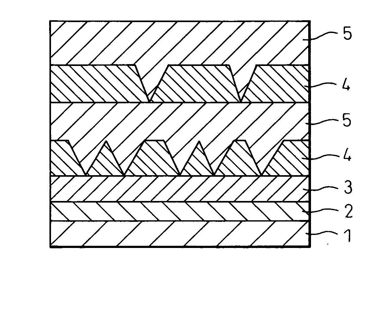
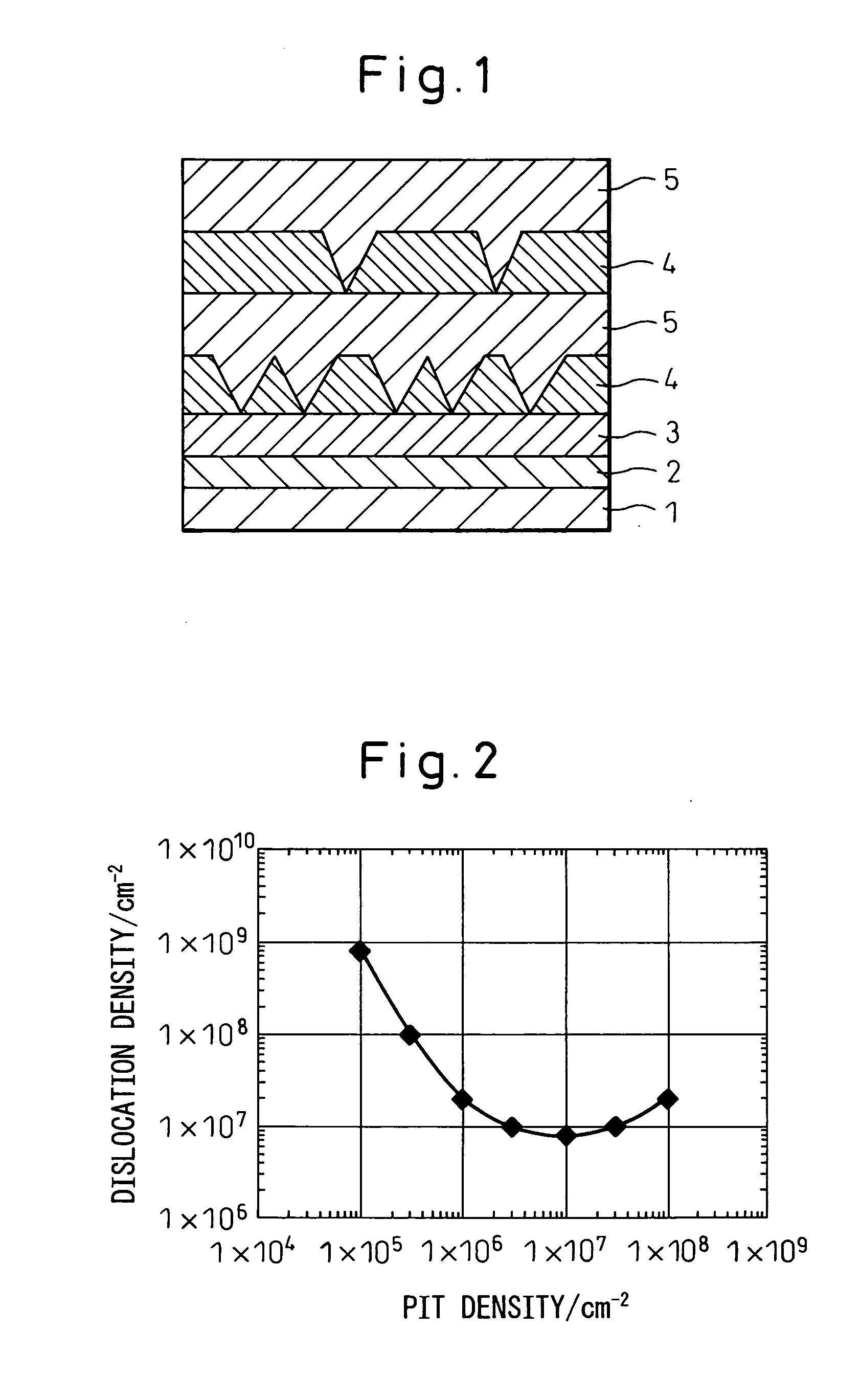
[0079]FIG. 1 is a view schematically showing the cross-sectional structure of the stacked structure for a Group III nitride semiconductor device, produced in this Example.

[0080] The structure where a Group III nitride semiconductor is stacked on a substrate comprising sapphire is formed through the following procedure by utilizing a general reduced-pressure MOCVD technique. First, a substrate 1 comprising (0001)-sapphire was placed on a susceptor made of a high-purity graphite for a semiconductor, which is heated to a film-forming temperature by a high frequency (RF) induction heating-type heater. Thereafter, a nitrogen gas was flowed into the stainless steel-made vapor phase growth reaction furnace to purge the inside of the furnace.

[0081] After flowing a nitrogen gas into the vapor phase growth reaction furnace over 8 minutes, the induction heating-type heater was actuated and the temperature of the substrate 1 was elevated from room temperature to 600° C. in 10 minutes. While k...

example 4

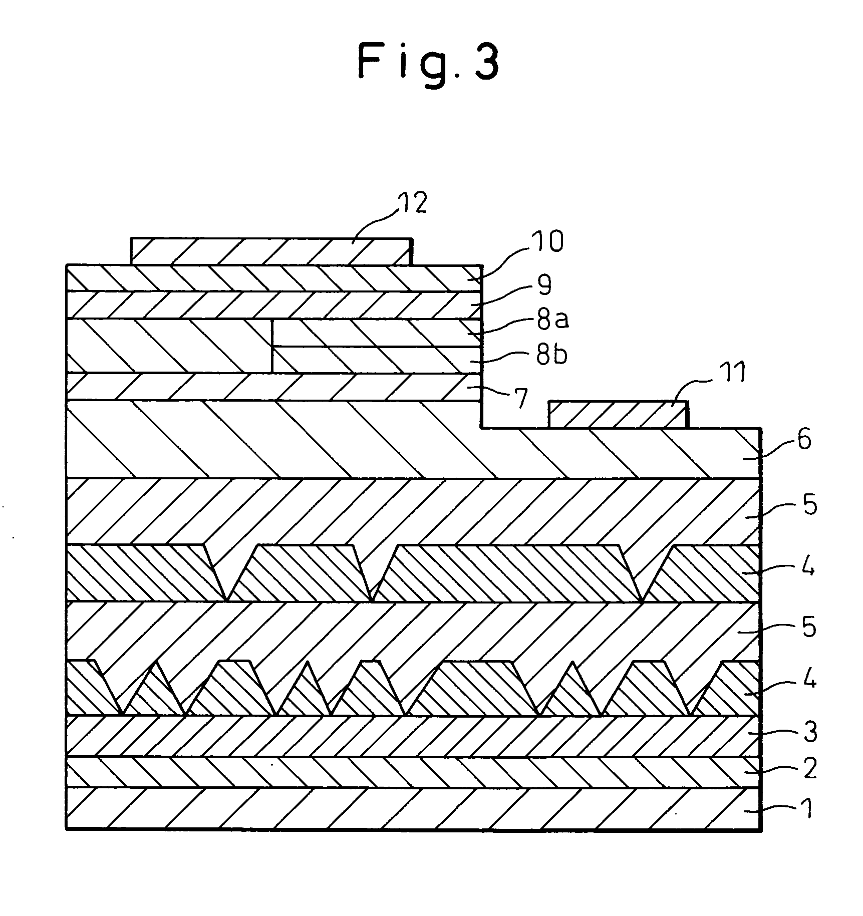
[0091] A Group III nitride semiconductor light-emitting device was produced by further stacking a Group III nitride semiconductor layer on the stacked structure produced in Example 1. FIG. 3 is a view schematically showing the cross-sectional structure of the Group III nitride semiconductor light-emitting device produced in this Example.

[0092] The procedure until the formation of the low-concentration impurity atom layer 5 was the same as that in Example 1. Thereafter, an n-contact layer 6 comprising Ge-doped GaN was stacked thereon at 1,120° C. and an n-clad layer 7 comprising undoped In0.03Ga0.97N was then stacked at 1,060° C. The thickness of the n-clad layer 7 was 12.5 nm. As for the n-contact layer 6 having a structure that a high-concentration Ge atom layer and a low-concentration Ge atom layer were alternately stacked in a repetition of 100 times, the total layer thickness was 2 μm.

[0093] Subsequently, the substrate 1 temperature was lowered to 730° C. and a multiple quantu...


PUM


Abstract

An object of the present invention is to provide a Group III nitride semiconductor stacked structure with a low dislocation density obtained by stacking only a semiconductor layer on a flat substrate by the use of a normal epitaxial growth method without processing the substrate or a deposit layer on the substrate, wherein the dislocation density is 1×107 cm−2 or less. The inventive Group III nitride semiconductor stacked structure comprises a substrate having a surface roughness (Ra) of 1 nm or less and a Group III nitride semiconductor layer directly stacked on the substrate, wherein the Group III nitride semiconductor layer comprises a plurality of layers put into contact with each other, the plurality of layers comprise a high-concentration impurity atom layer and a low-concentration impurity atom layer, and the high-concentration impurity atom layer is present on the substrate side.

Description

CROSS REFERENCE TO RELATED APPLICATION [0001] This application is an application filed under 35 U.S.C. §111(a) and claiming benefit, pursuant to 35 U.S.C. §119(e)(1), of the filing date of the Provisional Application No. 60 / 679,978 filed on May 12, 2005, pursuant to 35 U.S.C. §111(b).TECHNICAL FIELD [0002] The present invention relates to a Group III nitride semiconductor stacked structure, and a Group III nitride semiconductor light-emitting device using the same. BACKGROUND ART [0003] A Group III nitride semiconductor formed on a substrate has been heretofore used as a functional material for fabricating a Group III nitride semiconductor light-emitting device with a pn-junction type structure capable of emitting visible light at a short wavelength, such as a light-emitting diode (LED) and a laser diode (LD) (see, for example, Japanese Unexamined Patent Publication (Kokai) No. 2000-332364). For example, at the fabrication of an LED emitting near ultraviolet light, blue light or gre...

Claims


Application Information

Patent Timeline
IPC IPC(8): H01L33/00H01L33/32
CPCH01L33/32H01L33/025
Inventor BANDOH, AKIRA
Owner TOYODA GOSEI CO LTD
Why Eureka
Try Eureka