Process for forming a low carbon, low resistance metal film during the manufacture of a semiconductor device and systems including same

a metal film, low carbon technology, applied in semiconductor devices, semiconductor/solid-state device details, capacitors, etc., can solve the problems of unusable oxidizing byproducts such as metal tetraoxide not being produced, and achieve the effect of reducing contamination, reducing oxidation of exposed layers, and improving the conductivity of completed metal layers

Inactive Publication Date: 2006-11-23
MICRON TECH INC
View PDF10 Cites 33 Cited by
  • Summary
  • Abstract
  • Description
  • Claims
  • Application Information

AI Technical Summary

Benefits of technology

[0008] The present invention provides a method for annealing a metal layer which results in the formation of a highly conductive metal layer having reduced contamination and reduced oxidation of exposed layers. In accordance with one embodiment of the invention a pure metal layer, particularly a metal which does not form a metal nitride, is formed in accordance with previous methods such as chemical vapor deposition (CVD) or atomic layer deposition (ALD). Metals which do not form metal nitrides include ruthenium, cobalt, platinum, and nickel. The pure metal layer is then annealed in the presence of ammonia (NH3), borane (BH3), diborane (B2H6), hydrogen gas (H2), or carbon monoxide (CO). Annealing the completed metal layer as described densifies the metal, possibly by removing contaminants such as carbon, and improves the conductivity of the completed metal layer. Further, undesirable oxidizing byproducts such as a metal tetraoxide are not produced as these gasses are reducing and not oxidizing.

Problems solved by technology

Further, undesirable oxidizing byproducts such as a metal tetraoxide are not produced as these gasses are reducing and not oxidizing.

Method used


Image

  • Process for forming a low carbon, low resistance metal film during the manufacture of a semiconductor device and systems including same
  • Process for forming a low carbon, low resistance metal film during the manufacture of a semiconductor device and systems including same
  • Process for forming a low carbon, low resistance metal film during the manufacture of a semiconductor device and systems including same

Examples


Embodiment Construction

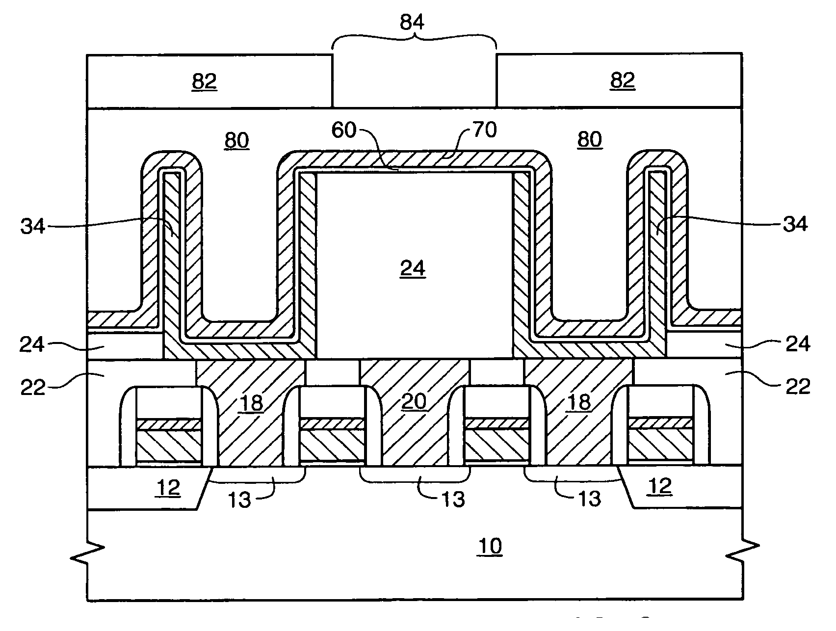
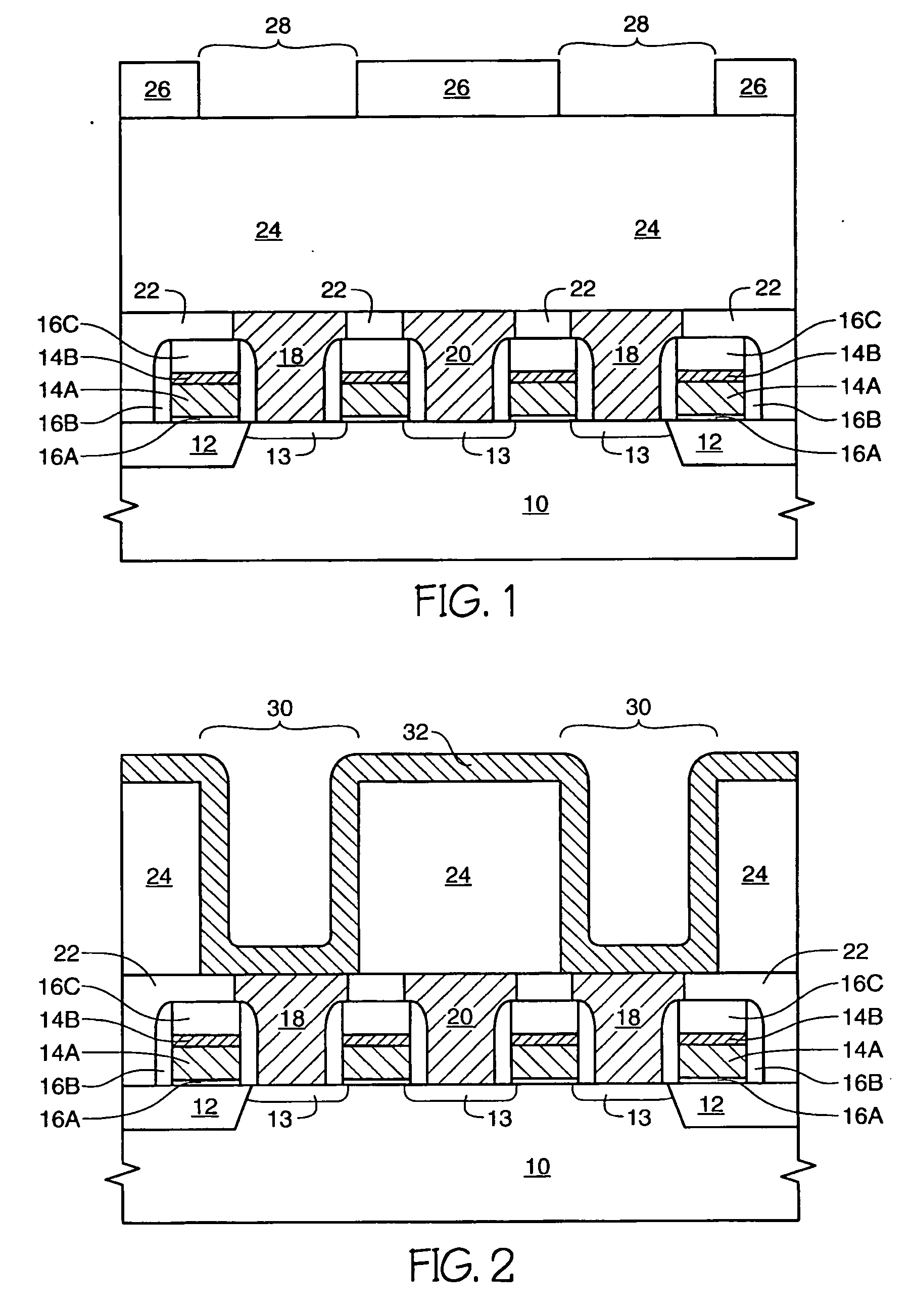
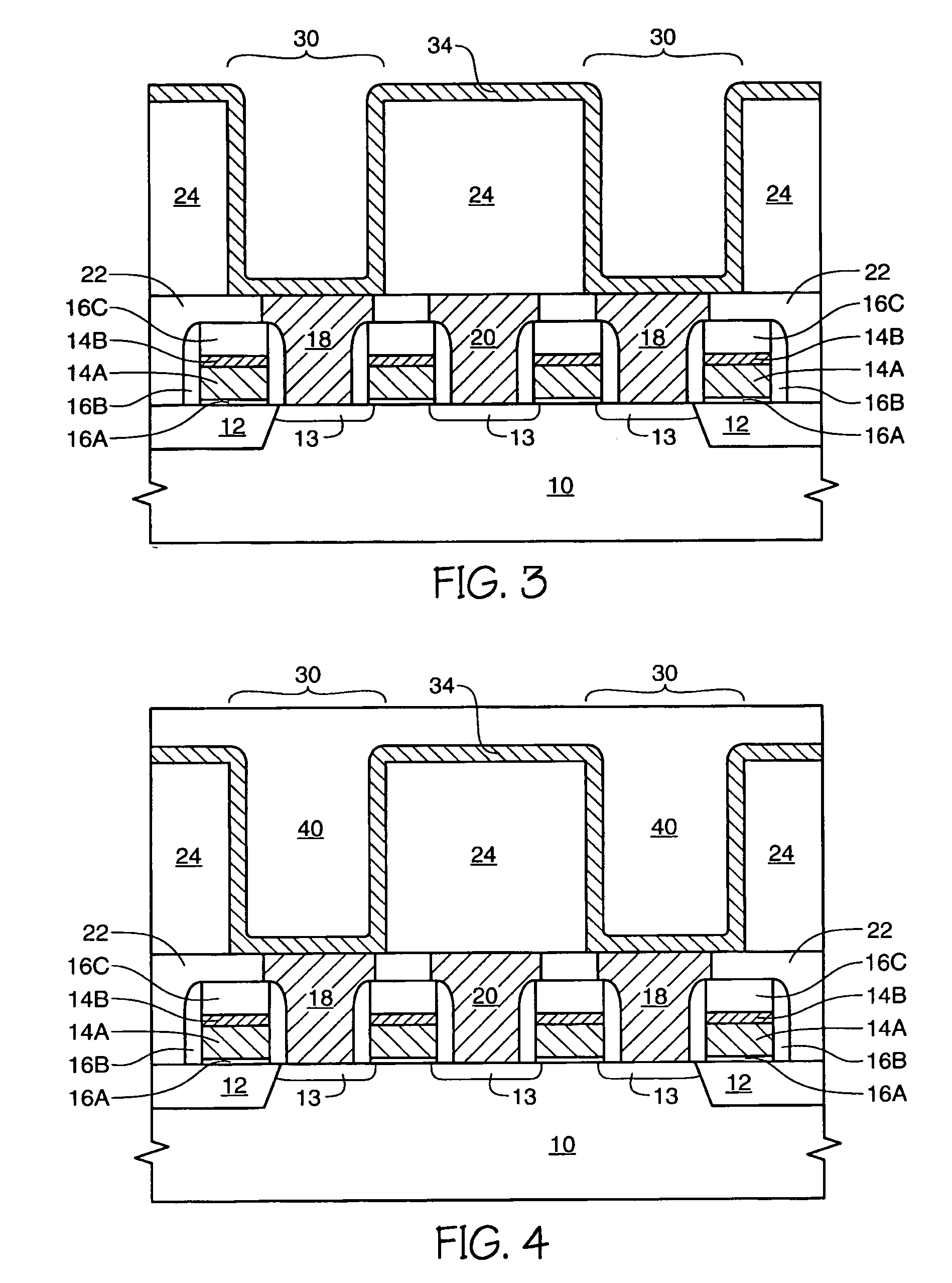
[0015] The term “wafer” is to be understood as a semiconductor-based material including silicon, silicon-on-insulator (SOI) or silicon-on-sapphire (SOS) technology, doped and undoped semiconductors, epitaxial layers of silicon supported by a base semiconductor foundation, and other semiconductor structures. Furthermore, when reference is made to a “wafer” in the following description, previous process steps may have been utilized to form regions or junctions in or over the base semiconductor structure or foundation. Additionally, when reference is made to a “substrate assembly” in the following description, the substrate assembly may include a wafer with layers including dielectrics and conductors, and features such as transistors, formed thereover, depending on the particular stage of processing. In addition, the semiconductor need not be silicon-based, but could be based on silicon-germanium, silicon-on-insulator, silicon-on-sapphire, germanium, or gallium arsenide, among others. ...


PUM

PropertyMeasurementUnit
temperatureaaaaaaaaaa
pressureaaaaaaaaaa

Abstract

A method for forming a conductive feature comprises forming a metal film such as ruthenium then annealing the film in an atmosphere comprising a hydrogen-rich gas such as ammonia, hydrogen, borane, or diborane, or in another gas such as carbon monoxide. The anneal may decrease the carbon content of the film and results in a metal layer having a lower resistance than the preannealed metal film.

Description

FIELD OF THE INVENTION [0001] This invention relates to the field of semiconductor manufacture and, more particularly, to a method for annealing a metal film which decreases the film's resistance and also may decrease the carbon content of the metal. BACKGROUND OF THE INVENTION [0002] Many different types of materials are used in the manufacture of semiconductor memory devices, logic devices, microprocessors, etc. Pure metals are becoming more commonly used in semiconductor manufacture for a wider range of purposes due to the prohibitively high resistance found with nonmetals and metal-containing compounds such as polysilicon, metal silicides, and metal nitrides, particularly with decreasing feature sizes. For example, attempts have been made to manufacture capacitor plates, typically formed from polysilicon, from ruthenium metal. Ruthenium may also be used as a barrier layer to copper migration and as a seed layer for copper plating. [0003] While the formation of a conformal metal ...

Claims


Application Information

Patent Timeline
Patent Type & Authority Applications(United States)
IPC IPC(8): H01L29/40H01L21/44
CPCH01L21/28556H01L21/76841H01L21/76862H01L21/76864H01L28/91H01L27/10811H01L27/10817H01L27/10852H01L28/65H01L21/76871H10B12/312H10B12/318H10B12/033
Inventor MARSH, EUGENE P.KRAUS, BRENDA D.
Owner MICRON TECH INC
Why Eureka
Try Eureka